Chinese semiconductor thread II

tokenanalyst

Lieutenant General
Registered Member

EDA tool company Hexin Technology completes a new round of financing.​

Anhui Hexin Technology Co., Ltd. (hereinafter referred to as "Hexin Technology") officially announced the completion of a new round of financing. This round of financing was jointly invested by Hefei Industrial Investment and Heno Capital, and the specific amount was not disclosed. The funds invested will be mainly used to expand the R&D team, accelerate the iteration of STA tool products, expand the customer base for AI high-computing power chips, and continue to promote the self-sufficiency of high-end timing verification EDA tools.
1784759276477.png

EDA is hailed as the "mother machine" of the integrated circuit industry. Static timing analysis (STA) is an indispensable core link in the back-end chip approval process. It has long been monopolized by overseas manufacturers, and there is an urgent need for domestic substitution.

Public information shows that HeXin Technology was founded in July 2023, with its headquarters located in Baohe District, Hefei City. HeXin Technology is a domestic supplier of fully stacked, independently controllable EDA tools focusing on the field of AI high-performance computing chips and specializing in static timing analysis (STA). It is also one of the few domestic EDA hard-technology companies that are fully self-developed, adaptable to advanced processes, GPUs, and AI acceleration chips, and have achieved complete self-development of core timing signature algorithms. Its core product, HeXin Timer, is optimized for AI computing chip PPA, relying on self-developed implicit circuit modeling and delay calculation algorithms to balance computational efficiency and timing accuracy.

The core team of Hexin Technology comes from leading international semiconductor companies such as Synopsys and Intel, and has world-class experience in EDA and high-end chip timing verification R&D.

Please, Log in or Register to view URLs content!
 

tokenanalyst

Lieutenant General
Registered Member

SmartSens launches 50-megapixel 0.61μm pixel-size CMOS image sensor for mobile phone applications.​

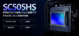
SmartSens, a leading CMOS image sensor supplier, officially launched its new 50-megapixel 0.61μm pixel size CMOS image sensor for mobile applications—the SC505HS. Based on SmartSens' SmartClarity® - 3 technology platform, the SC505HS features patented SFCPixel® technology , boasting advantages such as low power consumption, high sensitivity, Sparse PDAF® phase detection autofocus, and ULP mode. The SC505HS balances excellent imaging performance with cost advantages, bringing a comprehensively upgraded imaging experience to the main camera, front camera, and ultra-wide-angle applications of mainstream smartphones.​

1784818378594.png

Please, Log in or Register to view URLs content!
 

tokenanalyst

Lieutenant General
Registered Member

Dayang Bio’s Xinzhichun High-Purity Ceramics Project Enters Trial Production


Zhejiang Xinzhichun Semiconductor Materials Co., Ltd., a subsidiary in which Dayang Bio holds a 30% stake, has advanced its semiconductor-grade high-purity ceramic product project to the trial production stage. Initial products have been sampled and are currently undergoing verification by downstream customers.​
  • Project Specifications:
    • Investment & Size: 240 million yuan total investment, covering ~40 mu (26,702 sq meters of land) with a building area of 19,253.1 sq meters.​
    • Technology: Equipped with advanced machinery, including high-purity silicon carbide deposition furnaces, precision CNC machining centers, and fully automated cleaning lines.​
    • Capacity: Projected to produce 63,100 pieces/sets annually at full capacity, aiming to bridge domestic technological gaps in high-end semiconductor consumables.​
Founded in December 2023, Xinzhichun specializes in the R&D and industrial application of silicon carbide coating technologies (graphite-based coatings and solid silicon carbide materials via CVD) for semiconductor and LED epitaxial equipment. High-purity silicon carbide ceramics are critical consumables in semiconductor manufacturing, a sector historically dominated by imports. While this milestone marks significant progress in Dayang Bio’s semiconductor new materials strategy, the industry's high entry barriers and long verification cycles mean no short-term bulk orders are expected. Future revenue will depend heavily on successful downstream customer certification.

Please, Log in or Register to view URLs content!
 

tokenanalyst

Lieutenant General
Registered Member

JCET Group plans to invest 7.8 billion yuan to build a packaging and testing factory, and has already established a wholly-owned subsidiary with 4 billion yuan in assets.​


On June 24, the company held a meeting and approved the proposed investment to establish a holding subsidiary to build a high-end advanced packaging and testing factory in Wanxiang Industrial Park, "Oriental Chip Port" in Lingang, Shanghai. The total investment of the project is RMB 7.8 billion, and the registered capital of the proposed subsidiary is expected to be RMB 4 billion.

To advance the project, the company has completed the registration of its wholly-owned subsidiary and obtained its business license. This subsidiary is Changrun Microsystems (Shanghai) Co., Ltd., with a registered capital of RMB 400 million and Zheng Li as its legal representative.

Please, Log in or Register to view URLs content!
 

tokenanalyst

Lieutenant General
Registered Member

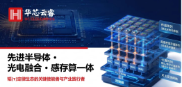
Huaxin Yunrui, a company specializing in optical chips, has completed its angel round of financing.​


Suzhou Huaxin Yunrui Microelectronics Technology Co., Ltd. announced the completion of an angel round of financing worth tens of millions of RMB. This round of investment was jointly led by WaNiu Capital and Shanda Investment, with participation from Suzhou Industrial Park Leading Venture Capital.

According to the company's disclosure, the funds raised will be primarily invested in the tape-out of optical interconnect and optical computing chips, and the engineering of integrated sensing, storage, and computing chips. They will also be used to expand the core R&D team, build a pilot production supply chain, and advance product reliability verification and market delivery, helping the company move from the cutting-edge technology R&D stage to productization, large-scale production, and industrialization. Subsequent funding will continue to be allocated to key areas such as product engineering, supply chain construction, verification testing, and market delivery.
1784819323121.png
Public information shows that Huaxin Yunrui Microelectronics was established based on the university-industry-research system, focusing on the research and development of fourth-generation semiconductor materials, optical computing, optical interconnects, and integrated sensing-memory-computing chips. Its technologies are geared towards application scenarios such as AI computing power and edge intelligent sensing. Optical interconnects and optical computing technologies are regarded as important routes to break through the bandwidth and power consumption bottlenecks of traditional electrical interconnects, while integrated sensing-memory-computing chips can reduce data transfer losses in AI terminals and adapt to the needs of edge devices and intelligent hardware.​

1784819227601.png

Please, Log in or Register to view URLs content!
 

tokenanalyst

Lieutenant General
Registered Member

Gewu Optics SOA Series Products: Domestically Produced Core Optical Devices


Gewu Optics' semiconductor optical amplifier series covers the 1270nm–1550nm wavelength band and offers various forms including bare chip, COC, and butterfly package, suitable for applications such as optical communication amplification, fiber optic sensing, LiDAR, and OCS switching matrices. Click to view the complete product list and customization options:

1550nm Butterfly-Packaged SOA

This product adopts a sealed inorganic encapsulation, integrates TEC thermoelectric cooling and temperature monitoring, has an operating temperature of -10~70℃, a storage temperature of -40~85℃, and an airtightness of 1×10⁻¹² Pa·m³/s, making it suitable for long-term operation in harsh environments.

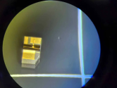
1270nm SOA Chip


1784821800976.png

This chip is extremely small and can be directly integrated with silicon waveguides, detectors, and other on-chip systems, providing crucial support for high-density photonic integration. Gewu Optics has achieved full domestic independent control over its chip manufacturing process and supports customized configurations such as polarization maintaining, integrated isolators, and integrated PD optical power monitoring.

Four major system-level advantages: Why is SOA indispensable for OCS?

Nanosecond-level ultra-fast scheduling


MEMS optical switches have a switching time of 1-10ms due to mechanical movement, while thermo-optical switches have a switching time of tens of microseconds. SOA is entirely based on carrier injection/extraction, with a switching time of <1ns. The overall switching latency of a 256-port OCS can be controlled within 100ns, which is 4-5 orders of magnitude faster than MEMS solutions. For the frequent full-representation communication in AI training, nanosecond-level switching significantly reduces synchronization waiting time and improves the effective computing power utilization of the cluster.

Built-in gain compensation to eliminate cascade losses

Passive optical switches have an insertion loss of 2-3 dB per stage, and a total loss of 8-12 dB for a 16×16 CLOS network, resulting in severe signal attenuation and requiring an external EDFA amplifier. SOA switches, on the other hand, provide 15-30 dB gain in the on-state and can be designed with a net gain >0 dB per stage. Multi-stage cascading does not reduce signal power but rather increases it, eliminating the need for external amplifiers, simplifying the system and reducing costs.

Ultra-low crosstalk and ultra-high reliability

SOA has an extremely high absorption coefficient in the off-state, achieving >50dB isolation (crosstalk <10⁻⁵) and ensuring a bit error rate of less than 10⁻¹² for 400G signals. It is entirely solid-state with no mechanical parts, and has a mean time between failures (MTBF) exceeding 500,000 hours.

Chip-level integration and low cost

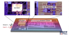
SOA utilizes III-V semiconductor processes (InP/InGaAsP, etc.) and can be heterogeneously integrated or bonded with silicon photonics platforms. A 16×16 OCS is only the size of a palm, one-tenth the size of a traditional electrically switched ASIC. Mass production capabilities compatible with CMOS processes continue to reduce the cost per port, driving the adoption of OCS from hyperscale data centers to edge nodes.

1784821894445.png


From the Ministry of Industry and Information Technology positioning optoelectronic chips and OCS devices as the foundation for artificial intelligence development, to OFC 2026 clearly defining OCS as the core architecture of next-generation data centers, all-optical switching is ushering in a golden age of industrialization. According to Cignal AI's forecast, the OCS market size will exceed $3 billion by 2029, with a compound annual growth rate of 58% from 2026 to 2029.

SOA, with its nanosecond-level switching speed, built-in gain compensation, and chip-level integration, has become the "super-powerful heart" of OCS all-optical switching. Over the next three years, SOA+OCS will continue to make breakthroughs in three main areas:​
  • Speed: Evolving from 800G to 1.6T and 3.2T​
  • Scale: Expanding from 32×32 to 128×128, 256×256, and even 1000 ports.​
  • Integration: Heterogeneous integration of SOA arrays and optical interconnect chips to construct higher-density all-optical interconnects​
Please, Log in or Register to view URLs content!
 

tokenanalyst

Lieutenant General
Registered Member

Fuzhou Chengxin Optoelectronics high end optical components meet the Parameter Requirements of DUV (Deep Ultraviolet) Semiconductor Equipment.​

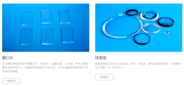
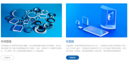
Deep ultraviolet (DUV) optical components are critical for semiconductor inspection systems operating at wavelengths of 193nm, 248nm, and 266nm. These components enable the resolution of minute defects in the 50–200 nm range through applications such as wafer defect AOI, mask inspection, film thickness measurement, and dark-field imaging. According to Fuzhou Chengxin Optoelectronics, meeting the rigorous demands of these applications requires strict adherence to specific material and optical parameter standards to leverage the short-wavelength diffraction limit effectively.

Only two primary substrate types are viable for high-end DUV applications:​
  • UV-Synthesized Fused PhotoLithography-Grade Silica (JGS1):
    • Use Case: 248nm/266nm systems and low-end 193nm paths.​
    • Pros: High mechanical strength, moisture-proof, easier to polish, moderate cost.​
    • Cons: Weak intrinsic absorption at 193nm; prone to color centers under long-term high-power irradiation (mitigated by raw material purification).​
    • Performance: >90% internal transmittance at 193nm (10mm thickness).​
  • PhotoLithography-Grade Calcium Fluoride (CaF₂):
    • Use Case: Preferred for high-end 193nm (ArF) objectives, windows, and polarizing prisms.​
    • Pros: Ultra-low dispersion, extremely low birefringence, >99.7% internal transmittance at 193nm.​
    • Cons: Prone to deliquescence (requires moisture-proof coating/packaging), low hardness, difficult to polish.​
    • Preference: <111> crystal orientation to minimize stress birefringence.​
  • Auxiliary: Magnesium Fluoride (MgF₂) is used for polarizer substrates and short-wavelength windows.​

Key Optical Parameters (Special Grade)

  • Surface Quality (Critical Threshold):
    • Accuracy: PV ≤ λ/10 to λ/50 @633nm (High-end starts at λ/50).​
    • Finish: Mil-0 standard (10/5 or 20/10) to suppress laser damage and scattering.​
    • Roughness: Ra ≤ 0.3–0.5nm to improve signal-to-noise ratio in dark-field imaging.​
  • Coating Systems (DUV-specific IBS Ion Beam):
    • AR Coating: Single-wavelength residual reflectance <0.25%; resistant to UV radiation.​
    • HR Coating: Reflectivity >97–99.5% using 35–45 layers of fluoride film.​
    • Durability: Laser Induced Damage Threshold (LIDT) >1.0–1.5 J/cm² (10ns pulse); transmittance drift <1% after 1 billion pulses.​
  • Polarization Components:
    • Wire Grid Polarizers: Extinction ratio >1000:1 (266nm) and ≥5000:1 (193nm custom).​
    • Prisms (GranTaylor/Wollaston): CaF₂ material with extinction ratio ≥10⁵:1 and beam deflection accuracy <1 arcminute.​
  • Objective Lens Imaging:
    • NA: 0.85–0.93 (dry) up to 1.35 (immersion).​
    • Resolution: Up to 80nm half-pitch.​
    • Wavefront Distortion: RMS < λ/20.​
  • Uniformity & Purity:
    • Refractive index uniformity at 1–5 ppm level.
    • Strict control of bubbles, inclusions, and point defects meeting photolithography-grade standards.
Chengxin Optoelectronics emphasizes rigorous incoming material screening and specialized processes (such as moisture-proof coatings for CaF₂ and purification for silica) to meet these demanding specifications. They offer both standard series products and customized solutions for various semiconductor inspection scenarios.

1784826018804.png1784826248243.png


Please, Log in or Register to view URLs content!
 
Top