Is quite an advancement but they still have work to do. probably a few years more.
The webpage states that the article was generated by AI.

Is quite an advancement but they still have work to do. probably a few years more.
by the founder with ai toolThe webpage states that the article was generated by AI.
I know the company and have seem the patents. they have been working in this light source for years.The webpage states that the article was generated by AI.
Extreme ultraviolet semiconductor provides a capillary discharge electrode ultraviolet lithography dual vacuum light source device
Suzhou Extreme Ultraviolet Semiconductor Co., Ltd. provides a capillary discharge electrode ultraviolet lithography dual vacuum light source device, which relates to the field of extreme ultraviolet lithography light source technology. It aims to solve the problem of light noise caused by the generation of electrode debris and tube wall debris during ceramic capillary discharge. The technical solution includes a capillary and electrodes. Electrodes are also provided at both ends of the capillary. A discharge chamber is also provided on the outside of the capillary. The discharge chamber is provided with a collection hole and an observation hole. The capillary is connected to a gas supply system.
- China Lighting Network
2024/5/13
21376
This improved the output power of extreme ultraviolet light, allowing for a lower discharge repetition frequency to meet the requirements of extreme ultraviolet lithography production; it significantly reduced electrode debris, tube wall debris, and light source impurities, which is beneficial for the output of extreme ultraviolet light; the use of a pneumatic system for air supply improved the purity of the extreme ultraviolet light; and the extension of the capillary length and the adoption of a side collection method greatly increased the collection surface compared to traditional end-face collection, thus increasing the collection efficiency of extreme ultraviolet light.

Oh didn’t know Naura was state owned. Impressive
I think Naura is a publicly traded company. SASAC has an stake in the company.Oh didn’t know Naura was state owned. Impressive
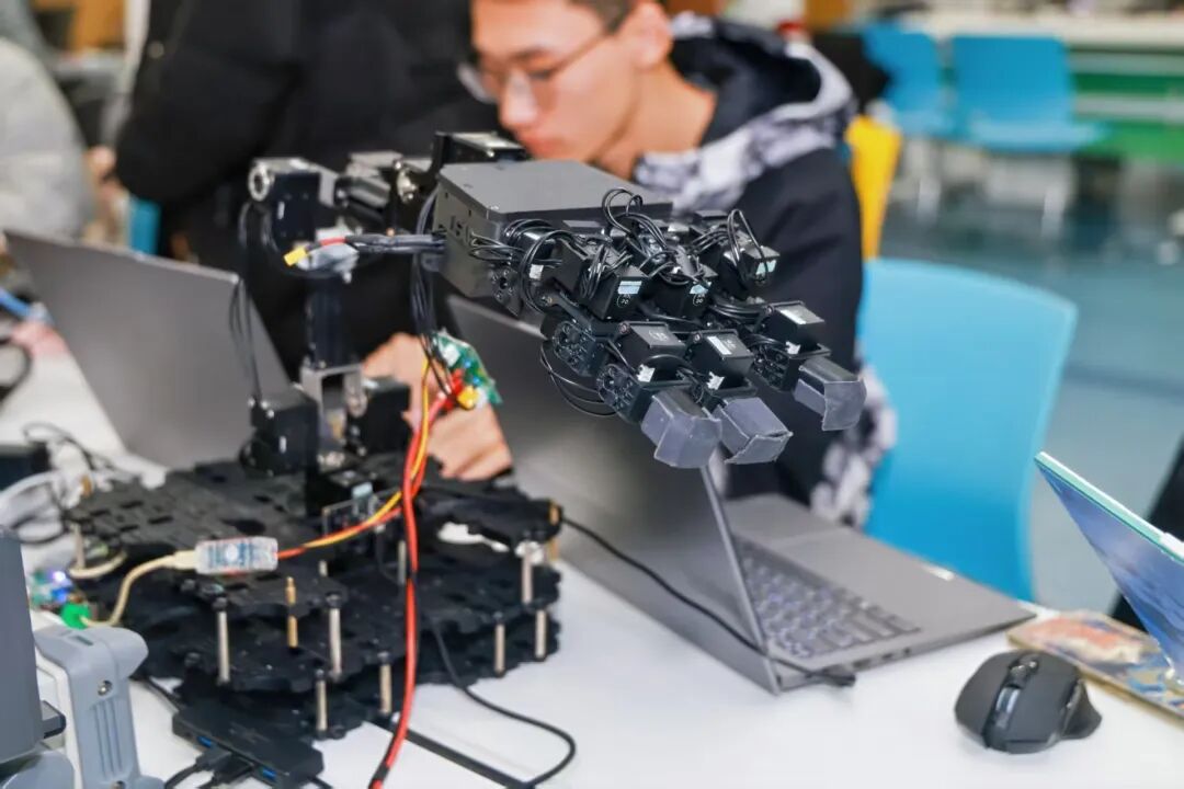
I came to this kind of late, but it is quite interesting they are talking about large scale FPGA using advanced FinFET. That means at least 14/12 nm process, if not even better. And also high precision ADCs. Has a lot of advanced applications here on radar and EW.
Anlu Technology plans to raise 1.262 billion yuan to increase its investment in the research and development and industrialization of high-end FPGA chips.
On January 26, Anlogic Technology unveiled its "2026 Plan for Issuance of A-Shares to Specific Targets," aiming to raise up to RMB 1.26 billion by issuing no more than 120.25 million shares—capped at 30% of pre-issuance share capital—to no more than 35 institutional investors. The funds will be used exclusively for two core R&D projects to strengthen its position in high-end field-programmable gate array (FPGA) chips and accelerate domestic technological substitution.
The issuance price will be set at no less than 80% of the average stock price over the previous 20 trading days, with all proceeds paid in cash and subject to a six-month lock-up period. After deducting issuance costs, the funds will be allocated as follows:
Gowin Semi/高云半导体 said it started mass producing new generation 22nm medium to high density FPGA chips.
Gowin Semi/高云半导's software 云源软件V1.9.12 have received TUV certification ASIL-D. Now fully support its 22nm advanced FPGA product. Its 55nm, 22nm product can be used in auto electronics, industrial control and such.
Jingsheng Electronics: Net profit for 2025 is expected to increase by 181.97%–192.21% year-on-year.
View attachment 168941
Jingsheng Electronics is forecasted to achieve a remarkable year-on-year increase in net profit of 181.97% to 192.21% for 2025, with attributable profits expected to reach RMB 80–90 million. This surge is driven by the company’s strategic pivot toward domestic semiconductor equipment substitution, particularly in metrology technologies for advanced semiconductor processes. The firm has successfully transitioned from heavy R&D investment into tangible commercialization, with key products such as film thickness measurement, OCD, and electron beam inspection equipment now achieving large-scale mass production. These advancements have significantly boosted delivery capacity and revenue recognition, while improved operational efficiency and a stronger business mix have propelled profitability across its semiconductor segment.
View attachment 168940
The company’s leadership in China’s semiconductor metrology market is underscored by its progress in advanced nodes: core products have already been successfully deployed at the 7nm process level, with verification underway for even more advanced nodes. Notably, its bright-field optical defect inspection equipment has received client acceptance at both 14nm and 28nm nodes, signaling strong adoption in cutting-edge manufacturing. As advanced process products now constitute a growing share of revenue and orders, they have become the primary engine of Jingsheng’s financial performance. The firm is capitalizing on China’s broader push for semiconductor self-reliance, positioning itself as a critical domestic supplier in a sector undergoing rapid technological and industrial transformation.
Beyond semiconductors, Jingsheng Electronics is also benefiting from a recovery in the flat panel display industry, fueled by expanded production lines—particularly G8.6 LCD and medium-to-large OLED facilities driving demand for its testing equipment. Leveraging deep customer relationships and technological expertise, the company is expanding its footprint in traditional display markets while venturing into emerging areas such as precision optical instruments and automotive electronics. This diversification, coupled with a streamlined customer and product portfolio, has led to a substantial order backlog and a marked improvement in gross margins. With both semiconductor and display segments delivering strong growth, Jingsheng Electronics is poised for sustained expansion, reflecting confidence in its technology-driven business model and the broader industrial upgrade trajectory in China.
Wafer-level integration of nanomaterials and MEMS sensing chips facilitates the industrialization of high-performance gas sensors.
Professor Guotao Duan’s team at the School of Integrated Circuits, HUST, has pioneered a groundbreaking wafer-level manufacturing process that seamlessly integrates nanomaterials with 3D MEMS sensing structures overcoming a decades-old industrial bottleneck in high-performance gas sensor development.
The team’s novel “film-first, cantilever-later” approach decouples nanomaterial synthesis and patterning from MEMS fabrication, enabling liquid-surface self-assembly of nanoparticles (e.g., Pd/SnO₂) onto 8-inch wafers with uniform, dense monolayers without damaging pre-fabricated microstructures. Key innovations include:
View attachment 168983
Published in Nano-Micro Letters (first author: Zheng Zhang, 2025 PhD graduate), this work provides the first complete, scalable manufacturing pathway for nanomaterial-enhanced MEMS gas sensors paving the way for mass production and industrial deployment in IoT, safety monitoring, and environmental sensing applications.
