Chinese semiconductor thread II

huemens

Junior Member
Registered Member
Please, Log in or Register to view URLs content!

China limits Nvidia chip purchases to special circumstances, Information reports​


The report about requiring upfront payment have also flipped

Nvidia says no upfront payment needed for its H200 chips​

Please, Log in or Register to view URLs content!
Jan 13 (Reuters) - Nvidia does not require upfront payment for H200 chips, a spokesperson for the U.S. chipmaker said in a statement to Reuters on Tuesday.
The company said it "would never require customers to pay for products they do not receive", in a response to a Reuters story on January 8 about the company having imposed unusually stringent terms requiring full upfront payment from Chinese customers seeking its artificial intelligence chips.
 

tokenanalyst

Lieutenant General
Registered Member
Please, Log in or Register to view URLs content!

芯碁微装's WLP series of product is already helping multiple advanced packaging factories to mass produce CoWoS-L products. Expects to enter mass production in 2026H2. Its WLP series has > 100m RMB of order.
CFMEE is advancing pretty quickly in the field of maskless lithography, probably the most successful one in more than a decade, along with Mikoptic, in 2014 this technology was seen more something for the lab rather to be use semiconductor manufacturing and packaging.

Please, Log in or Register to view URLs content!
 

sunnymaxi

Colonel
Registered Member
South korea tried this but didn't succeed.

Hubei Longzhong Laboratory: China's first boron carbide ceramic focusing ring successfully developed

the focusing ring is an important component placed outside the wafer and in direct contact with it. By applying voltage to the ring to focus the plasma passing through it, the plasma is focused onto the wafer to improve the uniformity of the process.

New Generation Long-Life Boron Carbide Ceramic Focusing Ring Technology for Chip Etching " focuses on the focusing ring, a key component of core etching equipment in semiconductor manufacturing. It has developed a new generation of long-life boron carbide ceramic focusing rings, which improves the resistance to reactive ion etching by 30%.

According to Li Bin, associate researcher at Hubei Longzhong Laboratory, they have successfully developed the first new generation of long-life boron carbide ceramic focusing rings for etching machines in China . This achievement improves etching resistance by 30% and has a service life of more than 30 days , which is significantly better than the mainstream silicon carbide focusing rings (15-20 days). At the same time, it maintains excellent thermal stability and mechanical properties, and the technology has reached the international leading level .

Please, Log in or Register to view URLs content!
 

sunnymaxi

Colonel
Registered Member
With a purity exceeding 99.99995%! CETC breakthrough in ultra-high purity graphite technology with domestic equipment.

Shanxi Zhongdianke Company, a subsidiary of China Electronics Technology Equipment Group Corporation (CETC), recently overcame the technical difficulties in purifying ultra-high purity graphite powder. Its self-developed horizontal purification equipment achieved a significant breakthrough, achieving a purity exceeding 99.99995%, providing strong technical and equipment support for the stable supply of ultra-high purity graphite.

134923_098236_newsimg_news.jpg


In addition to significantly improving purity, this process, through continuous parameter optimization, can reduce the production cost per kilogram to 40% of that of traditional methods, minimizing production costs while maximizing loading capacity. Currently, this process has achieved mass production, with stable performance, and has received high praise from customers.

It possesses the capability to research and develop and manufacture high-temperature purification and silicon carbide/tantalum carbide CVD (coating) series equipment, as well as the industrialization verification capability for carbon-based material purification/coating.

company already designated a national-level specialized and innovative "little giant".

Please, Log in or Register to view URLs content!
 

tokenanalyst

Lieutenant General
Registered Member

North China Electronics Group assists the Integrated sensing, storage, and computing chip "Made in Yizhuang"​


Recently, Beijing Xiling Vision Technology Co., Ltd. (hereinafter referred to as "Xiling Vision"), a company located in the Beijing Economic-Technological Development Area (Beijing Yizhuang), announced that its collaborative research project with the team led by Lin Longyang of Southern University of Science and Technology and Ruike Microelectronics, titled "A 55nm Intelligent Vision SoC Achieving 346TOPS/W System Efficient via Fully Analog Sensing-to-Inference Pipeline," based on ReRAM (Resistive Random Access Memory) , has been officially accepted by the IEEE International Solid-State Circuits Conference (ISSCC) 2026, the world's top semiconductor academic conference. ISSCC is known as the "Olympics of Chips" and is the most authoritative academic forum in the global solid-state circuit field. This acceptance signifies a leading international breakthrough in novel in-memory computing architecture, end-to-end intelligent vision processing, and ultra-low-power integrated circuit design.

Addressing the energy efficiency bottlenecks of traditional edge AI vision systems caused by the separation of sensing and computing and frequent analog-to-digital (A/D) conversions, this research innovatively proposes a fully analog-domain intelligent vision architecture. The chip deeply integrates a ReRAM in-memory computing array with the image sensing unit, constructing a continuous analog signal processing path from perception and feature extraction to inference, completely eliminating the cumbersome A/D conversion overhead between the sensor and the computing layer. This design achieves true end-to-end "sensing-memory-computing integration," successfully overcoming the dual constraints of computing power and power consumption, and providing a highly competitive next-generation solution for power-sensitive intelligent terminal fields such as edge AI, micro-robotics, and autonomous driving.

It is worth noting that this research achievement also benefited from the mature integrated circuit industry ecosystem of the Beijing Economic-Technological Development Area (BDA). During the research and verification process, the team fully utilized BDA's professional equipment and supply chain resources in the semiconductor manufacturing field, and received strong support from Naura Technology Group and Beijing Zhanrui Technology Co., Ltd., demonstrating the complete industrial synergy advantages of BDA's integrated circuit industry, from design, equipment, manufacturing to packaging and testing.

XiLing Vision, a high-tech chip company dedicated to developing next-generation intelligent vision sensors and intelligent optoelectronic sensors, has achieved groundbreaking technological innovation through its "In-Pixel Computation" technology. This technology, refined and iterated over many years, surpasses the traditional von Neumann architecture, efficiently combining pixels and cores to deliver unparalleled speed, low power consumption, and intelligence compared to traditional architectures. The products focus on edge processing applications, providing complete intelligent vision sensor solutions from 2D to 3D.

Please, Log in or Register to view URLs content!
 

tokenanalyst

Lieutenant General
Registered Member

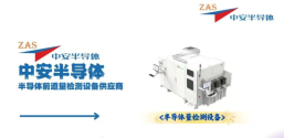
Zhong'an Semiconductor patternless wafer particle inspection equipment


In 2024, Zhong'an Semiconductor officially released a patternless wafer particle inspection equipment, targeting the needs of mainstream process nodes. Its minimum detection sensitivity reaches 26nm. In September of the same year, Zhong'an further launched an advanced particle inspection equipment that can fully cover 14nm/10nm process node applications. This series of equipment has been tested and verified at multiple customer sites, demonstrating excellent detection capabilities and process adaptability.

In 2025, Zhong'an Semiconductor officially launched its new generation of high-sensitivity particle detection equipment, achieving another breakthrough in minimum sensitivity, suitable for the most advanced manufacturing process nodes in China. Zhong'an has achieved comprehensive coverage from mature to advanced processes, and can broadly meet the core needs of customers at different process nodes in terms of process monitoring, yield improvement, and process optimization.

1768344626900.png

Looking to the future, Zhong'an plans to launch a metrology solution for more advanced process nodes in 2026, continuously expanding its technological boundaries and providing the integrated circuit industry with higher precision and more efficient testing and measurement support.​
 

tokenanalyst

Lieutenant General
Registered Member

Effect of electric field configuration on EUV-induced plasma dynamics​

Abstract​

The configuration of external electric fields generated by electrostatic chucks plays a critical role in plasma dynamics during extreme ultraviolet lithography, yet the underlying coupling mechanisms remain incompletely understood. This study employs first-principles particle-in-cell simulations to investigate how the field topology of electrostatic chucks and the location of EUV irradiation regulate the kinetics of a transient hydrogen plasma. Results demonstrate that strong fields of electrostatic chucks govern the plasma dynamics by controlling the evolution of the space potential, which in turn regulates charged particle energy distributions and surface bombardment characteristics. Specifically, symmetric bipolar electrodes establish a global potential gradient that promotes sustained ion acceleration and broadens the electron energy distribution. In contrast, pitch-shaped electrodes produce a localized periodic field that predominantly affects near-surface particle dynamics. These findings clarify the key coupling mechanisms between electric field geometry and EUV-induced plasma behavior, offering vital insights for mitigating plasma-induced damage and improving process stability in lithography systems.

Please, Log in or Register to view URLs content!
 

tokenanalyst

Lieutenant General
Registered Member
"The School of Materials Science and Engineering focuses on strengthening close ties with the semiconductor industry in the field of extreme ultraviolet lithography. Through close cooperation with photoresist companies such as Tongcheng Microelectronics and Beijing Kehua, chip design and manufacturing companies such as Huawei HiSilicon, Changxin Memory, SMIC, and IMEC of Belgium, semiconductor equipment companies, and large scientific facilities such as the Shanghai Synchrotron Radiation Facility, the team focuses on key materials, processes, and equipment for advanced semiconductor processes at the sub-2nm process node"

The 2nm supply chain is taking form.​
 
Top