Chinese semiconductor thread II

tokenanalyst

Lieutenant General
Registered Member

The Zonghui Xingguang high-end optical communication chip project with a total investment of 550 million yuan was completed and put into production​

According to the official Weibo of Wujin today, on the morning of September 10, the Zonghui Xingguang high-end optical communication chip project with a total investment of 550 million yuan was completed and put into production in Wujin National High-tech Zone. The project is dedicated to the research and development and manufacturing of high-end compound semiconductor chips.

The newly-commissioned project covers an area of 40 mu and has a construction area of 28,000 square meters. After reaching full production capacity, it will form large-scale production capacity for gallium arsenide and indium phosphide chips.
Founded in 2015, Zonghui Xingguang is an optoelectronic semiconductor company dedicated to providing customers with high-performance vertical-cavity surface-emitting laser (VCSEL) chips and modules, optical communication laser chips, and radio frequency epitaxial wafers. The company primarily develops and produces VCSEL chips, high-speed optical communication chips, devices, and modules, with applications in consumer electronics, 3D sensing, virtual reality, augmented reality, autonomous driving, biomedical sensors, and high-speed optical communications.

The application scenarios of VCSEL laser chips are rapidly expanding with the development of 3D perception, autonomous driving, artificial intelligence and other fields, and the market demand for high-performance, high-reliability, and high-speed high-end VCSEL laser chips has increased dramatically.

In 2019, Zonghui Xingguang achieved breakthroughs in epitaxial growth technology for key semiconductor materials, becoming the first company in China to achieve mass production of VCSELs. By August 2023, the company had shipped 100 million VCSEL chips and expanded into the automotive electronics and optical communications sectors. To date, Zonghui Xingguang has completed 11 rounds of financing, backed by over 20 renowned VC/PE and industrial investors, including Huawei, Xiaomi, BYD, DJI, Hesai Technology, RoboSense, Wuyuefeng Capital, Gaorong Capital, and Glory Ventures, raising over 2 billion yuan in total.

Please, Log in or Register to view URLs content!
 

jx191

New Member
Registered Member
The post you reference says that picture was from July 2024. The problem is despite all the rumors and such in the past years there still hasn't been any actual production. I understand that tight OPSEC means we probably won't get official notice of anything but if these systems were ready then we should see it in the actual output of wafers. Right now it seems they are still not ready for production and given tight OPSEC it's just really hard to tell how far along they actually are. That's the part that I think frustrates me and a lot of other people, there's just no way to know how far along DUV and EUV are and when actual production will happen.


I don't really see why they would make it public. I'm very doubtful that USA response to China getting their own machines would be to say "well I guess sanctions didn't work, we give up." Rather the predictable result would be even more sanctions from USA. So in that context it's much more likely they keep everything quiet as there's no real benefit to openly announcing it.
Well let's wait until production starts ramping up for advanced nodes during next year. Then we can talk about "actual production." At least for DUV.

But like tphuang said, it's best if we leave the speculation and move on for now.
 

tokenanalyst

Lieutenant General
Registered Member

Big Fund Phase III Tuojing Technology Industrial Project.​


The announcement shows that Tuojing Technology plans to issue shares to specific objects to raise a total amount of no more than RMB 4.6 billion, which will be used for the construction of a high-end semiconductor equipment industrialization base and a cutting-edge technology R&D center, of which RMB 1.1 billion will be invested to supplement working capital.

Among them, the high-end semiconductor equipment industrialization base construction project focuses on the expansion of thin film deposition equipment. It is planned to build a new industrialization base in Hunnan District, Shenyang, Liaoning Province, including production clean rooms, three-dimensional warehouses, testing laboratories, etc. It will introduce advanced production supporting software and hardware to create a large-scale, intelligent and digital high-end semiconductor equipment industrialization base.

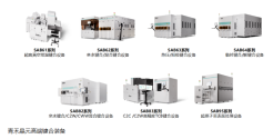
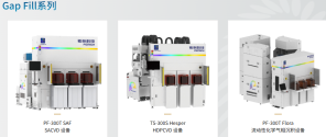
According to reports, the project plans to invest 1.768 billion yuan, with a construction period of five years. Tuojing Technology claims that the implementation of this project will significantly increase the company's high-end semiconductor equipment production capacity, supporting the industrialization of its thin-film deposition equipment series, including PECVD, SACVD, and HDPCVD. Through the construction of intelligent supporting facilities, it will improve production efficiency, fully meet the needs of downstream markets and customers, expand the company's business scale, and further enhance the company's competitiveness and market position.

1757693901895.png


The construction project of Tuojing Technology's cutting-edge technology research and development center focuses on the development of advanced process equipment and plans to invest 2 billion yuan.

Tuojing Technology stated that through the implementation of this project, the company plans to carry out research and development of a number of advanced thin film deposition equipment, including PECVD, ALD, trench filling CVD and other process equipment, and gradually break through the cutting-edge core technologies, thereby forming a series of products with independent intellectual property rights; at the same time, it will continue to optimize and upgrade PECVD, ALD, trench filling CVD and other products to meet the iterative needs of advanced processes.

Please, Log in or Register to view URLs content!
 

tokenanalyst

Lieutenant General
Registered Member

Sunking Technology and Sanan Semiconductor have reached a strategic cooperation​


On September 12, 2025, Sunking Technology announced that its wholly-owned subsidiary, Sunking Asia Pacific Semiconductor Technology (Zhejiang) Co., Ltd., and Hunan San'an Semiconductor Co., Ltd., have signed a strategic cooperation framework agreement, establishing a comprehensive strategic partnership. This collaboration aims to leverage both parties' technological and industrial strengths in semiconductors, particularly power devices, to promote collaborative development and achieve mutual benefit.

Sunking Semiconductor specializes in the R&D and manufacturing of power semiconductor devices. San'an Semiconductor, a wholly-owned subsidiary of San'an Optoelectronics, boasts a vertically integrated manufacturing platform covering the entire silicon carbide (SiC) industry chain. Its 8-inch SiC chip production line has already achieved mass production and is now online. In this partnership, San'an Semiconductor will ensure a stable and timely supply of Sunking products based on Sunking Semiconductor's needs, and will grant Sunking Semiconductor priority supply in its production plans.

Both parties expressed their intention to jointly assess future market growth potential, develop capacity expansion plans, and engage in resource sharing and technology exchange to further enhance their market competitiveness. Sunking Technology hopes that this strategic partnership will strengthen its competitive advantage in the global semiconductor industry, particularly in the power device market.

Please, Log in or Register to view URLs content!
 

tokenanalyst

Lieutenant General
Registered Member

Unigroup Guoxin releases China's first automotive-grade LPDDR4x chip to boost the development of intelligent connected vehicles​


The first domestic automotive-grade LPDDR4/LPDDR4X product launched by Unigroup Guoxin . It has now completed AEC-Q100 certification and entered the mass production stage. It is widely used in key control units of intelligent connected vehicles.

Product model 1: SCE11U64324EF-04ZA2
Maximum speed: 4266 Mbps
Capacity options: 2/4/6/8 GB
Bit width: x32
Operating temperature: Meets automotive Grade 2 (-40~105℃) or Grade 3 (-40~95℃) requirements
Application areas: Intelligent cockpit CDC, central control unit CCU

Product model 2: SCB11N8G322BF-04ZA2
Maximum speed: 4266 Mbps
Capacity options: 4/8 Gb
Bit width: x32/x16
Operating temperature: Meet automotive Grade 1 (-40~125℃) or Grade 2 (-40~105℃) requirements
Application areas: LiDAR, front-view cameras, DMS, CMS, AR-HUD, central gateway, VDC
This series of products meets automotive-grade requirements in terms of interface design, power consumption control, and reliability. They can maintain stable operation in complex environments and meet the high-bandwidth, low-power storage requirements of intelligent driving and advanced driver assistance systems (ADAS).

Please, Log in or Register to view URLs content!
 

tphuang

General
Staff member
Super Moderator
VIP Professional
Registered Member
Please, Log in or Register to view URLs content!

Largest OSAT companies in China as of 2024

长电科技:全球第三、国内第一,2024年营收360亿元,遥遥领先。2025年上半年2.5D/3D封装收入同比+217%,XDFOI平台实现5层RDL、线宽/线距2μm,拿下英伟达、AMD、华为昇腾910B等高端订单;上海临港车规级基地通过IATF16949认证,目标锁定汽车Chiplet。


通富微电:AMD“御用”封测厂,2024年营收239亿元。VISionS平台融合2.5D/3D/MCM-Chiplet,3D NAND堆叠良率>90%,TSV成本较海外低40%;联合CXMT开发HBM,5nm已量产验证。

华天科技:2024年营收143亿元,汽车电子封装特色鲜明,双面塑封BGA-SiP、uMCP已量产;12英寸晶圆级TSV产线聚焦CIS、MEMS,良率85%,但2.5D/3D仍处第二梯队。
JCET, Tongfu and Huatian account for > 77% of China's market share in 2024

2nd grouping are
芯德半导体:36μm凸点间距打破垄断,RDL-interposer方案获BroadPak技术奖;扬州基地30万片/年产能2025年5月投产,专攻2.5D。

云天半导体:玻璃基板多层RDL堆叠,TGV 60μm/200μm、线宽1.5μm,中介板尺寸2700mm²,为AR/VR、毫米波雷达提供大尺寸方案。

湖南越摩:控股股东兴橙资本打通“EDA/IP+12吋厂+玻璃基封装”全链;与京东方合作GPU玻璃基样品,2026年望进入小批量。

Hchiplet绍兴项目:一期30亿元,年产200万颗AI Chiplet,锁定GPU/CPU异质集成。
I have not heard of this 2nd group of companies. Look like they specialize in different areas

资本层面,国家大基金三期明确将先进封装列入重点;深圳、上海、绍兴等地政府产业基金同步跟进,2025年行业融资规模已突破600亿元,为产能扩张提供“弹药”。
 

PopularScience

Senior Member
Registered Member
The Ministry of Commerce website released two announcements on September 13, initiating anti-dumping investigations on imported analog chips originating in the United States and anti-discrimination investigations on relevant measures taken by the United States against China in the field of integrated circuits.

Please, Log in or Register to view URLs content!
 

tokenanalyst

Lieutenant General
Registered Member

Qinghe Jingyuan, solving the problem of optoelectronic integration with advanced bonding technology!​


At the High-Performance Optoelectronic Integrated Chip Frontier Technology Forum, Group Deputy General Manager Liu Fuchao delivered a special report titled "Advanced Bonding Technologies for Optoelectronic Convergence: Material Innovation and Device Integration." The presentation provided an in-depth analysis of the core challenges and development trends facing current bonding technologies, focusing on the innovative applications of various advanced bonding technologies in optoelectronic device integration and photonic chip packaging. These forward-looking industry insights are based on Qinghe Jingyuan's technological breakthroughs and industrialized practices in the field of optical-microelectronics convergence. The practical solutions proposed in the presentation provide a clear path to addressing the industry's core pain points.

Dr. Guo Chao, Deputy General Manager of the Group, delivered a keynote speech titled "Advanced Bonding Technologies for CPO and Heterogeneous Integration." He systematically expounded on the development trends of CPO technology and the new requirements it places on the bonding process. He highlighted breakthroughs in hybrid bonding technology in addressing key challenges such as bubble control, strength uniformity, bonding accuracy, and thermally induced diffusion and stress. He also shared Qinghe Wafer's technological advantages and industrialized cases in ultra-high vacuum room-temperature bonding and heterogeneous material integration, providing innovative solutions for CPO and heterogeneous integration from a practical application perspective.

Deepening industrial collaboration and creating a future ecosystem together

In response to the special needs of the optoelectronic integration field, Qinghe Jingyuan demonstrated a number of distinctive technologies:
● In response to the heat dissipation needs of high-power lasers, we launched ultra-high vacuum room temperature bonding technology to significantly reduce the interface thermal resistance
● Provide hydrophilic bonding solutions for silicon photonic chip integration to achieve low-loss optical path docking
● Develop hybrid bonding process for CPO packaging needs, supporting high-precision interconnection up to ±100nm
● Provide temporary bonding solutions for device thinning processing to improve process yield

1757778047659.png

Please, Log in or Register to view URLs content!
 
Top