Chinese semiconductor thread II

tokenanalyst

Brigadier
Registered Member

Machining of ultra- precision optical components are the core components of lithography machines, with extremely high barriers and high value tracks​


As the first research institute in the field of optics established in New China, Changguang Institute has undertaken the important task of making breakthroughs in lithography machines, and its technical strength is self-evident.

The processing of large-aperture optical lenses is the key to improving the resolution of optical lenses. The optical system has stringent requirements on the surface accuracy of the reflector. Changguang Institute has made breakthroughs in large-aperture magnetorheological polishing equipment and independently developed equipment to fully master the core processing technology. 1) In 2018, the 4.03-meter large-aperture silicon carbide reflector developed by Changguang Institute successfully passed the acceptance inspection. This is also the world's largest-aperture silicon carbide single reflector publicly reported; 2) It also has the research and development capabilities of a full set of manufacturing equipment required for the manufacture of reflectors. In addition, Changguang Institute's three core equipment, the 4-meter-scale reaction sintering furnace, the FSGJ-4 aspheric CNC optical processing center, and the 4-meter-scale large-scale magnetron sputtering coating machine, have all reached the domestic leading level.

Cooperated with Changguang Daqi to establish a joint venture company, and the ultra-precision processing capabilities were endorsed
Huachen Equipment and Changguang Optoelectronics have established a joint venture company, Changguang Huachen, in which the company holds a 72.7% stake. The company is responsible for the production of ultra-precision optical components , guide rails and other grinding machines, and provides related ultra-precision optical component processing. With the accelerated breakthrough of domestic substitution of lithography machines, the company has tied up with leading players, and its business is expected to develop rapidly
1751992536941.png
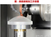
Looking at the details of the cooperation specifically, the processing process of the lithography machine lens is complicated. On the one hand, the company provides grinding equipment as a technical verification, and on the other hand, it provides the key front-end milling and grinding link of the lens embryo.
1751992304652.png

1) Front-end process: The mirror blank is first milled and formed by a high-precision machine tool to ensure the initial completion of the mirror shape and curvature. The processing accuracy needs to be controlled at the nanometer level;
2) Use a small grinding head to polish

magnetorheological polishing, ion beam polishing and other ultra-precision polishing methods to eliminate defects and coat the film. The company's front-end milling and grinding link directly determines the efficiency and time of the subsequent processes.​
 

gelgoog

Lieutenant General
Registered Member
Last edited:

gelgoog

Lieutenant General
Registered Member
IMHO the talk about "Huawei affilliated" fabs is BS. Thus far there is no evidence of that. Huawei just use regular Chinese foundries and chip suppliers. Huawei have their own fab for optoelectronics chips but that is about it.
 

tokenanalyst

Brigadier
Registered Member

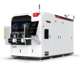
Nashe's intelligent fully automatic dual-chamber 8-inch silicon carbide epitaxial equipment is delivered!​

In the summer of 2025, Nashe Intelligent has made a key progress - the self-developed fully automatic dual-chamber 8-inch silicon carbide epitaxial equipment and multiple 8-inch single-chamber equipment have been delivered to leading customers! This milestone marks that the company's product strength in the field of third-generation semiconductor equipment has entered a new stage, injecting new innovative power into the cost reduction and efficiency improvement of the global silicon carbide industry chain.​

1752072052765.png

Technological breakthrough

Seize the opportunity of 8-inch industry upgrade


With the surge in demand for silicon carbide devices in scenarios such as new energy vehicles and ultra-high voltage charging piles, the global industry is accelerating its upgrade to 8-inch wafers. With its independent and controllable technical core, Nashe Intelligent is the first to achieve mass production and delivery of 8-inch equipment. Since its launch, the company's 8-inch equipment has won repeat purchases from major customers several times, confirming the market's recognition of the company's product strength.

Empowering industries

The technology ecosystem continues to expand


From the shipment of the first silicon carbide epitaxial equipment in 2021 to the delivery of the 8-inch dual-chamber epitaxial equipment this time, Nashe Intelligent has always been "committed to becoming a global leader in advanced material manufacturing equipment." In 2025, the new generation of intelligent epitaxial systems will integrate automation technology to promote the evolution of advanced material equipment and equipment towards "high efficiency, low carbon, and intelligent integration."

From single-chamber breakthroughs to dual-chamber leadership, Nashe Intelligent responds to the proposition of the times with hard-core innovation. The batch delivery of 8-inch equipment is a testament to our technological strength and a firm commitment to upgrading the global industrial chain. In the future, we will continue to work with our partners to shape the intelligent future of the silicon carbide industry!


Please, Log in or Register to view URLs content!
 

tokenanalyst

Brigadier
Registered Member
IMHO the talk about "Huawei affilliated" fabs is BS. Thus far there is no evidence of that. Huawei just use regular Chinese foundries and chip suppliers. Huawei have their own fab for optoelectronics chips but that is about it.
In the case of China, absence of evidence is not evidence of absence. Huawei is pretty much getting in the semiconductor industry and patents give a hint of that. They probably already have fabs for some processes and chips like RF, power and logic chips. While collaborating with SMIC for the most advance chips.
 
Last edited:

tokenanalyst

Brigadier
Registered Member
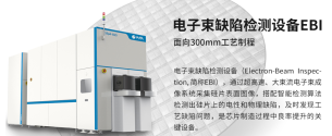
DJELX launched it first HV-SEM.

Oriental Crystal Source appeared at the 2025 Jiwei Semiconductor Conference to showcase electron beam measurement and detection technology for advanced processes​


Key Product Launches & Technological Advancements
1. Next-Generation Electron Beam Defect Inspection (EBI): SEPA-i635

  • Enhanced Performance: Achieves 3x faster detection speed vs. predecessors (e.g., SEPA-i525).
  • Core Innovations:
    • Ultra-large current pre-charging (microampere-level) and large current imaging (hundred nanoampere-level) for detecting electrical defects in complex 3D structures on advanced memory wafers.
    • Beam current improved by an order of magnitude, validated by production-line testing.
  • Applications: Supports diverse scenarios, rivaling international advanced foreign equipment.
2. Electron Beam Defect Re-inspection (DR-SEM): SEpA-r655
  • Imaging Capabilities:
    • 5-channel electron imaging (4 side + 1 top detectors) for 3D defect visualization and material contrast analysis.
    • High depth-of-field imaging for high-aspect-ratio structures; millimeter-level field of view for wafer-edge analysis.
  • Additional Features:
    • DUV microscopy module for unpatterned wafer detection and automatic defect composition analysis.
    • Adaptive hardware for compound semiconductors and variable wafer thicknesses.
    • Autofocus hardware/software optimizations double inspection speed.
  • Recognition: Won the "Industrial Chain Breakthrough Award" at the Jiwei Semiconductor Manufacturing Summit.
3. Critical Dimension Measurement (CD-SEM): SEpA-c505
  • Performance Upgrades:
    • New high-speed film transmission platform for increased throughput.
    • Self-developed electron optical system (EOS) with improved resolution and measurement repeatability, matching international 12-inch CD-SEM standards.
  • User Experience: Intuitive software interface and support for advanced measurement algorithms tailored to sub-14nm processes.
1752078292889.png
4. High-Energy Electron Beam (HV-SEM): First Public Disclosure
  • Breakthrough Capabilities:
    • "Perspective" imaging to analyze deep wafer layers, measuring critical dimensions (HV CD), uniformity (CDU), and overlay accuracy (In-die SEM Overlay) for 3D-NAND, DRAM, and <14nm logic processes.
    • Self-developed EOS with 40KeV landing energy, achieving international parity.
  • Strategic Significance: Completes Dongfang Jingyuan’s comprehensive layout across four core front-end electron beam measurement areas, reinforcing its domestic leadership.
Please, Log in or Register to view URLs content!
 

tokenanalyst

Brigadier
Registered Member

New breakthrough! 4-inch ultra-thin and ultra-flat diamond film helps chip bonding and heat dissipation​


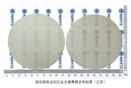
Recently, the functional carbon material team led by Jiang Nan, a researcher at the Ningbo Institute of Materials Technology and Engineering, Chinese Academy of Sciences, successfully prepared a 4-inch diamond self-supporting film with a thickness of less than 100 μm and a warpage controlled within 10 μm . This achievement not only broke the record in the field of diamond materials in China, but also marked a key step in the industrialization of "ultimate semiconductor" materials in China.

Technological innovation and major breakthroughs

Although traditional chemical vapor deposition (CVD) can grow diamond films, the thermal stress between the film and the substrate causes severe warping, and the thickness is difficult to break through the millimeter level. The Jiangnan team achieved a technological breakthrough through the independently developed " heteroepitaxy-laser lift-off-surface treatment " combined process. By optimizing the laser parameters, the lift-off energy consumption was reduced by 40%, and the lift-off time was shortened to less than 30 minutes, significantly improving production efficiency.

First, a high-quality single-crystal diamond film was grown on a sapphire substrate using heteroepitaxial technology, and then the film and substrate were precisely separated using laser energy, successfully controlling the film thickness below 100 μm and reducing the warpage to the international leading level. This thickness is only one-tenth of that of traditional diamond films, but it maintains excellent thermal conductivity (2200 W/m·K) and breakdown field strength (10 MV/cm) , far exceeding the performance of silicon and silicon carbide materials.

1752079007030.png

In addition, the team innovatively introduced the "surface gradient doping" technology to form a nanoscale doping layer on the surface of the film, effectively reducing the contact resistance. Test data showed that the contact resistivity of the film was 60% lower than that of the traditional process, laying the foundation for the manufacture of high-performance devices.

The transition of diamond materials from the theoretical value of ultra-high thermal conductivity to the actual process of mass production, packaging and bonding is becoming a consensus and goal, and is also the focus of competition in the next generation of chip thermal management technology. The successful development of diamond self-supporting film has taken a key step in overcoming the warpage problem that has long restricted the chip bonding process and promoting the development of diamond in the field of thermal management.​

Please, Log in or Register to view URLs content!
 

tokenanalyst

Brigadier
Registered Member
Looks like Huawei took a majority stake in the Shanghai based RF EDA company NineCube, expanding HiSilicon EDA capabilities.

As one of the few EDA tool providers in China with independent intellectual property rights, Jiutongfang has become a "Huawei-affiliated" company that has attracted much attention in the domestic EDA field since it received strategic investment from Huawei's Hubble Technology in 2020. Hubble Technology's investment not only provides financial support for Jiutongfang, but also injects momentum into its core technology research and development in the field of RF integrated circuit design.
1752079641396.png

Jiutongfang's equity structure shows that Huawei's Hubble Technology Venture Capital Co., Ltd. has become the largest shareholder, holding 11.1157% of the shares; National Integrated Circuit Industry Investment Fund II Co., Ltd. (Big Fund II) holds 7.781% of the shares and is the sixth largest shareholder; although the founders Wan Bo, Li Hong and Liu Minqing have withdrawn from direct shareholding, they indirectly hold 13.1325% of the shares through Wuhan Jiutongfang Enterprise Management Partnership.

At present, Jiutongfang's EDA tools have covered the entire process of RF IC design, including key links such as circuit simulation, layout design, and electromagnetic field analysis. Its core products can meet the high-precision design requirements of RF chips in high-end fields such as 5G communications, the Internet of Things , and automotive electronics. After this change, Jiutongfang's registered capital increased to 11.69941 million yuan, with 142 insured persons, and the company type changed to a limited liability company with investment from Hong Kong, Macao, and Taiwan, and non-sole proprietorship.

Industry insiders commented that the rise of Jiutongfang has filled the gap in the RF segment of domestic EDA and provided a possibility for breaking the technological monopoly of foreign manufacturers.

Please, Log in or Register to view URLs content!
 

tokenanalyst

Brigadier
Registered Member

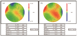
Absolute surface shape detection technology based on rotation-translation method and second-order derivative.​

Abstract​


Precise surface metrology is fundamental for quality control in manufacturing, particularly in fields such as space optics, ultrahigh-intensity ultrashort laser devices, free-electron lasers, and extreme ultraviolet (EUV) lithography. Achieving subnanometer accuracy in surface measurements is essential for manufacturing multifunctional, high-precision, and low-defect optical components. However, conventional interferometry, which relies on relative measurements, is limited by the quality of the reference flat, thus potentially reducing precision. Absolute measurement techniques have emerged as an effective solution for isolating and mitigating wavefront errors in both test and reference flats. This study proposes an advanced absolute-flatness measurement technique that combines the shift-rotation method with a second-order partial derivative algorithm. This approach is designed to enhance stability, reduce environmental error sensitivity, and simplify the experimental process while maintaining high accuracy. By expanding wavefront error analysis to second-order derivatives in polar coordinates, this technique offers improved robustness and applicability of large-aperture optical devices.

1752079986881.png

Please, Log in or Register to view URLs content!
 
Top