Chinese semiconductor thread II

tokenanalyst

Brigadier
Registered Member

Kaishitong delivered the first low-energy, high-beam ion implanter to a new customer in the sensor industry​


On June 13, Shanghai Kaishitong Semiconductor Co., Ltd. (hereinafter referred to as "Kaishitong"), a subsidiary of Wanye Enterprise, successfully delivered the first low-energy large-beam ion implanter to the first new customer in the sensor industry who won the purchase order through bidding. This achievement is not only a reaffirmation of Kaishitong's market competitiveness, but also a sign that Kaishitong has won customer recognition with its independent research and development and customization capabilities, injecting strong momentum into the development of domestic equipment serving the country's major strategies.
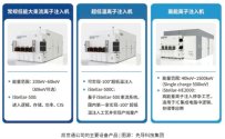
1750116646799.png

As the core interface between the physical world and the digital world, sensors are the foundation for the survival and development of all kinds of modern industries. After a thorough technical comparison, the customer chose Kaishitong. The key consideration was Kaishitong's industrialization capabilities that have been verified in large quantities and its excellent performance in key production lines. At the same time, based on its strong independent research and development and customized service capabilities, Kaishitong machines can better meet customers' personalized process needs and provide strong equipment support for customers' safe mass production.

With the rapid development of the semiconductor industry, Kaishitong will continue to be driven by technological innovation, guided by market demand, and aim at customer satisfaction, constantly improve its core competitiveness, serve customers' high-quality development with excellent equipment solutions, and help the country achieve high-level scientific and technological self-reliance.

Please, Log in or Register to view URLs content!
 

tokenanalyst

Brigadier
Registered Member
Why anyone would need such high refresh rate.

Domestic manufacturer SDC plans to launch 720Hz gaming monitor.​


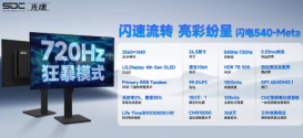
Chinese manufacturer SDC plans to launch a 720Hz WOLED 2K gaming monitor "Lightning 540-Meta", which will be the first to break the 700Hz refresh rate barrier for gaming monitors, with a brightness of up to 335 nits in SDR mode.

If the recent 600Hz gaming monitors from MSI and ASUS aren't fast enough for you, the SDC Optic Soul might just be the one to satisfy your high refresh rate cravings. This isn't your run-of-the-mill 360Hz or 500Hz gaming monitor, but a 720Hz monitor that might be the first to break the 700Hz barrier.

Chinese display manufacturer SDC has reportedly prepared a 720Hz WOLED gaming monitor. Unlike the 600Hz products from MSI and ASUS, it does not use a TN panel, and the current maximum refresh rate of OLED panels is 500Hz. ASUS and MSI have used Samsung's third-generation QD-OLED panels to launch flagship 2K@480Hz QD-OLED gaming monitors, while SDC's 720Hz gaming monitor will use LG's fourth-generation W-OLED panels.

1750116934369.png

Please, Log in or Register to view URLs content!
 

tphuang

General
Staff member
Super Moderator
VIP Professional
Registered Member
3nm chips and EUV is good and all but next gen semiconductors are going to upgrade defense weaponary.

Shandong University led the team to develop the "Chinese chip", and the domestic radar achieved "detecting the enemy first and defeating the enemy first"​

The National Key Laboratory of Crystal Materials and dean of the Institute of New Generation Semiconductor Materials of Shandong University. He has been forging the future of China's semiconductors in the microscopic world for twenty years.

Faced with long-term foreign technological blockades, "inability to grow, poor growth, and difficulty in processing" have become the three major obstacles in China's silicon carbide materials field, severely restricting the development of China's high-end equipment. The team decided to challenge this "Mount Everest of the semiconductor industry" starting from the most basic theory.

They solved the problem from the nucleation control theory, and innovated the energy level compensation and dislocation composite technology to transform the crystal growth from "blind men groping in the dark" to precise control. After thousands of process optimizations and parameter adjustments, the team finally achieved the leap from 2-inch to 12-inch single crystals - this is not only a simple size breakthrough, but also a disruptive innovation to traditional theories.

The team has conquered more than 40 core patents, formulated my country's first semi-insulating silicon carbide SiC military product standard, and built an independent and controllable technical barrier. What is more valuable is that the team insists on promoting technology implementation with industrial thinking, incubating companies listed on the Science and Technology Innovation Board through technology transfer, allowing "crystals in the laboratory" to move towards large-scale production, and bringing scientific research results out of the school and into society, injecting fresh vitality into the semiconductor industry, and making important contributions to the independent control of my country's key materials technology.

In the field of national defense, breakthroughs in silicon carbide are directly related to national security. The high-purity semi-insulating silicon carbide developed by the team has been successfully applied to the core components of phased array radars, increasing the detection distance by three time., From the J-20's airborne systems to cutting-edge weapons and equipment, this "Chinese core" carries the lifeline of national security. It allows Chinese radars to see farther, missiles to hit more accurately, and laser weapons to be more powerful, becoming an indispensable "hard-core shield" in national defense science and technology.

The breakthrough of silicon carbide is not only related to national defense, but also brings about changes in new energy and other fields. Facing the new energy industry, the team has made breakthroughs in the core technology of n-type silicon carbide manufacturing, providing underlying support for electric vehicles to solve the "range anxiety" and "charging bottleneck". This breakthrough not only helps my country's electric vehicle industry to "change lanes and overtake"
, but also reshapes the global third-generation semiconductor competition landscape and supports the backbone of China's high-end manufacturing.​
here is the casita article

Please, Log in or Register to view URLs content!

Very interesting that it increased detection distance by 3x. That is quite impressive. With military grade semi-insulating SiC wafer.
 

nativechicken

Junior Member
Registered Member
General MCU uses general registers internally and DSP uses floating point registers specialized in floating point calculation.

ISA is the bus.
For TI's DSP C2000 series solutions, China's National University of Defense Technology has developed the Feiteng DSP series (Feiteng includes separate branches for DSPs and CPUs). Most of these are compatible with or upgraded versions of the C2000 DSPs. Early models maintained compatibility with TI's DSP libraries, while later iterations reportedly outperformed the originals on that performance basis.

Essentially, China has developed pin-to-pin compatible chips for nearly all of America's top-tier military and civilian DSP chip series—some even supporting direct binary library compatibility.

Over the past five years, China has transitioned to fully independent R&D. Having exhausted feasible reverse-engineering options (largely excluding FPGAs), the focus is now entirely on original design innovation (with limited U.S. military chip upgrades to reference in recent years).

Currently in military/specialized chips, the primary gap remains FPGA technology, lagging by one or two generations. China has just crossed the threshold of single-chip FPGA designs exceeding a hundred million gates.
 

european_guy

Junior Member
Registered Member
Serving Large Language Models on Huawei CloudMatrix384

Interesting paper from Huawei.

Please, Log in or Register to view URLs content!

I post here because it has some official info on Ascend 910C

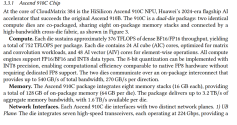
3.3.1 Ascend 910C Chip
At the core of CloudMatrix 384 is the HiSilicon Ascend 910C NPU, Huawei’s 2024-era flagship AI
accelerator that succeeds the original Ascend 910B. The 910C is a dual-die package: two identical
compute dies are co-packaged, sharing eight on-package memory stacks and connected by a
high-bandwidth cross-die fabric, as shown in Figure 3.
Compute. Each die sustains approximately 376 TFLOPS of dense BF16/FP16 throughput, yielding
a total of 752 TFLOPS per package. Each die contains 24 AI cube (AIC) cores, optimized for matrix
and convolution workloads, and 48 AI vector (AIV) cores for element-wise operations. All compute
engines support FP16/BF16 and INT8 data types. The 8-bit quantization can be implemented with
INT8 precision, enabling computational efficiency comparable to native FP8 hardware without
requiring dedicated FP8 support.
The two dies communicate over an on-package interconnect that
provides up to 540 GB/s of total bandwidth
, 270 GB/s per direction.
Memory. The Ascend 910C package integrates eight memory stacks (16 GB each), providing
a total of 128 GB of on-package memory (64 GB per die). The package delivers up to 3.2 TB/s of
aggregate memory bandwidth, with 1.6 TB/s available per die.

Network Interfaces. Each Ascend 910C die interfaces with two distinct network planes. 1) UB
Plane: The die integrates seven high-speed transceivers, each operating at 224 Gbps, providing a
total of 196 GB/s unidirectional (or 392 GB/s bidirectional) bandwidth to the scale-up UB plane.
2) RDMA Plane: Separately, each die includes a dedicated interface delivering up to 200 Gbps of
unidirectional bandwidth for the scale-out RDMA plane.

3.3.2 Ascend 910C Node
Each compute node in CloudMatrix384 integrates 8 Ascend 910C NPUs, 4 Kunpeng CPUs, and 7 UB
switch chips onboard, as illustrated in Figure 4. The 12 processors (8 NPUs and 4 CPUs) connect to
these on-board switches via UB links, creating a single-tier UB plane within the node. Each NPU is
provisioned with up to 392 GB/s of unidirectional UB bandwidth, while each Kunpeng CPU socket
receives approximately 160 GB/s of unidirectional UB bandwidth. An individual UB switch chip
onboard offers 448 GB/s of uplink capacity to the next switching tier in the supernode fabric.
Only NPUs participate in the secondary RDMA plane. Each NPU device contributes an additional
400 Gbps unidirectional link for scale-out RDMA traffic, yielding an aggregate of 3.2 Tbps of RDMA
bandwidth per node.
Within the CPU complex, the four Kunpeng CPU sockets are interconnected via a full-mesh
NUMA topology, enabling uniform memory access across all CPU-attached DRAM. One of the CPUs
hosts the node’s Qingtian card, a dedicated data processing unit (DPU) that not only integrates high-
speed network interfaces but also performs essential node-level resource management functions.
This Qingtian card serves as the primary north–south egress point from the node, interfacing with
the third distinct network plane: the datacenter’s VPC plane.
 

Attachments

  • 1750162555780.png
    1750162555780.png
    656.1 KB · Views: 9

huemens

Junior Member
Registered Member
Serving Large Language Models on Huawei CloudMatrix384

Interesting paper from Huawei.

Please, Log in or Register to view URLs content!

I post here because it has some official info on Ascend 910C

Ascend 910C Compared with H100:
- 24% less compute
- 60% more memory
- similar memory bandwidth
- 18% higher DeepSeek R1 throughput per TFLOP.

Despite less compute, because of higher token throughput efficiency on a per-TFLOP basis the overall performance is pretty good, at least for DeepSeek inference workloads.
DeepSeek R1 Prefill throughput is equal to 90% of H100 and Decode throughput is equal to 89.46% of H100.
 

tokenanalyst

Brigadier
Registered Member

Huawei's new "four-chip package" patent is exposed, which may be related to Ascend 910D​


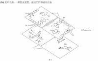
On June 17, according to foreign media Tom's hardware, Huawei recently applied for a "quad-chiplet" packaging design patent, which may be used for the next-generation AI accelerator Ascend 910D.
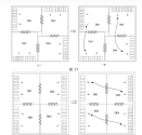
According to the information disclosed in the patent, the quad-chipset design is similar to NVIDIA's Rubin Ultra architecture. It uses advanced packaging technology to package four computing chips together, which is expected to significantly improve the overall performance of a single chip package. Although the patent document does not explicitly state that it is related to Huawei's new generation AI chip Ascend 910D, the previous generation Ascend 910C seems to be two Ascend 910Bs packaged together. Judging from recent industry rumors, it is highly likely related to Ascend 910D.
1750172652435.png
The patent content shows that the four chips are connected together using a technology similar to "bridging" (such as TSMC CoWoS-L or Intel EMIB with Foveros 3D), rather than a simple silicon interposer. At the same time, in order to meet the needs of AI training processors, multiple sets of HBM are also used to interconnect with the interposer.

Foreign media pointed out that although SMIC and Huawei are lagging behind in advanced manufacturing processes, their advanced packaging may be on par with TSMC. In this way, Chinese manufacturers can use older manufacturing processes to manufacture multi-chip processors, and then use advanced packaging integration to improve performance, which may narrow the gap with advanced process chips.

1750172673867.png
The Ascend 910B single chip area is about 665 square millimeters, and the Ascend 910D with four chipsets has a total chip area of 2,660 square millimeters. If each 910B is equipped with four HBM memories, then four groups of 16 HBMs will occupy an area of about 1,366 square millimeters. It is estimated that the entire Ascend 910D requires at least 4,020 square millimeters of silicon wafer area. If we look at it by TSMC standards, the current maximum size of the mask is about 858 square millimeters, which is equivalent to a total of five EUV mask sizes.
Although the outside world is mostly reserved about the Ascend 910D, it is now gradually supported by substantial evidence. Indeed, industry sources have pointed out that Huawei is developing the Ascend 910D quad-chipset processor, and the single chip package performance exceeds NVIDIA H100. In addition to the Ascend 910D, it is rumored that Huawei is also developing the Ascend 920 processor to compete with NVIDIA H200. However, the naming logic is still controversial and more information is needed.

Please, Log in or Register to view URLs content!
 

tokenanalyst

Brigadier
Registered Member

Yuntian Semiconductor's 3D Glass IPD mass production project delivers more than 10 million pieces​


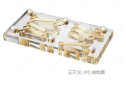
In the second quarter of 2025, the single mass production project of 3D Glass IPD designed by Shanghai Xinbo and manufactured by Yuntian Semiconductor delivered more than 10 million units, marking the realization of large-scale and stable output of the world's first 3D Glass IPD production line, injecting strong "core" power into fields such as AI, automotive electronics and IoT applications.

Compared with through silicon via (TSV) substrates, through glass via (TGV) substrates are favored by the market in passive device manufacturing due to their high resistivity, low dielectric loss, high thermal stability and adjustable thermal expansion coefficient. Yuntian uses glass as the substrate. Glass has a high resistivity greater than 10^12 Ω·cm and a dielectric loss tangent value of a few thousandths or even a few ten-thousandths. High-performance IPD devices are manufactured through the unique and stable 2.5D through glass via (TGV) metal interconnect technology and high-precision wiring layer process. They have excellent comprehensive performance in terms of device size, Q value, insertion loss, and out-of-band suppression. Thanks to Corewave's excellent design and Yuntian's advanced glass-based process platform, it has been successfully achieved that the performance of the N77 band filter is more than 20% higher than that of the silicon-based filter under the same size, providing a more competitive product solution for 5G RF modules.

1750172825763.png

It is estimated that the global thin-film IPD market will reach US$680 million in 2025. Driven by the deepening of 5G commercialization, automotive intelligence, and advanced packaging technologies (such as CoWoS), the glass-based IPD market is expected to have a CAGR (compound annual growth rate) of more than 10% in the next five years. With years of technological accumulation, Yuntian has cooperated with many customers to develop passive filters, high-performance inductors, capacitors and other devices, and its total delivery volume has accounted for more than 90% of the domestic market share. In particular, the N77/79 type IPD filter achieves ≤1.5dB in-band insertion loss, demonstrating its excellent signal processing capabilities.

Yuntian's new passive device production line has been put into operation since 2022. After three years of R&D verification and technical breakthroughs, it has achieved a double increase in production capacity and yield. The breakthrough in the delivery volume of 3D Glass IPD is not only an important milestone in the industrialization of Yuntian's IPD process platform, but also a testimony to the win-win cooperation with Shanghai Xinbo. Xinbo has more than ten years of development and design experience in the IPD field and is also a leading company in the design of 3D Glass IPD in the world. To commemorate the milestone of delivering 10 million pieces in a single 3D Glass IPD project, Yuntian Semiconductor held a delivery commemoration ceremony with the theme of "Tens of Millions of People with the Same Core, Working Together to Forge", and invited representatives of Xinbo and Yuntian employees to participate, to jointly remember the struggle of the 3D IPD project from R&D to mass production, and to look forward to higher and farther goals in the future.

Please, Log in or Register to view URLs content!
 
Top