Chinese semiconductor thread II

tokenanalyst

Brigadier
Registered Member

Experimental Study on the Inhibition of Carbon Transport and Deposition by Gas Lock Structure in Vacuum Chambers​


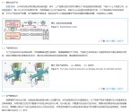
Abstract: Extreme ultraviolet lithography technology represents one of the most advanced semiconductor manufacturing processes. However, during this process, hydrocarbon compounds and water vapor are generated through material outgassing and photo-induced physical-chemical reactions, which can infiltrate the projection chamber and result in carbon deposition on multilayer mirrors' surfaces. This phenomenon significantly impacts product quality while also increasing costs associated with component replacement and maintenance. The introduction of clean gas via a gas lock structure effectively mitigates the diffusion process of pollutants, thereby offering a viable technical solution. In this study, simulation and orthogonal experiments were conducted to investigate the flow rate and temperature of clean gas as well as pollutants under different gas lock structures. The suppression rate parameters for pollutants by gas locks under varying process conditions were determined. These research findings provide a numerical basis for designing gas lock structures, selecting parameters for process experiments, and offer valuable insights into controlling pollution sources within similar vacuum environments.

1748533618805.png

Please, Log in or Register to view URLs content!
 

Wahid145

Junior Member
Registered Member
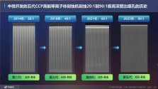
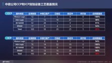
More on AMEC, looks like their ICP/CCP coverage continue to improve

Also, they are able to do 90:1 high aspect ratio CCP tool now, which I assume is what allows YMTC to do 200+ layer 3D NAND

View attachment 153145
View attachment 153146
Where Can I Find the PDF for these slides? Also anyone has updates on AMEC dive into Deposition tools? Looks like Etching is fully self sufficient in China right now. So many products from Naura too (etching)
 

PopularScience

Senior Member
Registered Member
AMEC boss

Please, Log in or Register to view URLs content!

4. If there is no EUV, it is no problem to use DUV lithography to achieve 5nm, but it will require more double and multiple exposure process steps for etching thin films, but it is still a question whether it can be done to 3nm. I believe in the ability and ambition of the Chinese people.
5. If the lithography machine cannot be solved quickly, what we can do in our main business of etching thin films is to combine the technology of multiple exposure to make the process smaller, which is also our responsibility.
 

tokenanalyst

Brigadier
Registered Member
More on AMEC, looks like their ICP/CCP coverage continue to improve

Also, they are able to do 90:1 high aspect ratio CCP tool now, which I assume is what allows YMTC to do 200+ layer 3D NAND

View attachment 153145
View attachment 153146
I think ratio of 100:1 can give you up to 1000 layers.

The 1,000-layer HAR etch challenge

When creating 3D NAND, essentially, the number of oxide and nitride layers determines the number of memory cells and thus the memory density and capacity of the device. Each vertical memory string begins with the creation of a cylindrical hole, which might be approximately 100nm in diameter and 5-6 µm deep (an aspect ratio of 50-60:1) and penetrate 128 layers.

The difficulty of etching very deep and precise high-aspect ratio (HAR) cylindrical holes only increases with the number of layers and the corresponding stack thickness. When hundreds of layers of ONON films are patterned to create holes with a critical dimension of 100-115 nm, this pushes the etched aspect ratio (depth/width) above 100:1.

“The depth of the hole relative to its diameter is now greater than 50 to 1,” Singh said. “As vertical scaling happens, the number of layers and hole depth is increasing, but the diameter generally has been held constant.” This means that 1,000-layer 3D NAND, comprised of multiple tiers, may require a hole with an aspect ratio of as much as 100:1. “This requires that the memory channel etch have atomic precision” he said.

reating such a high-aspect ratio hole at such small dimensions is hard to comprehend, especially when you consider that the “profile” of the hole must be near perfect from top to bottom, and, in production, a 100 trillion of them may be formed across a 300 millimeter wafer. Singh says that creating this highly precise channel shape is critical for vertical scaling, lateral scaling, and logical scaling (such as going from TLC to QLC and beyond).


LAM is using Cryogenic Etching for that.

The solution

One solution to creating a perfect cylinder, says Singh, is a pulsed power plasma technology developed by Lam that uses very high power in very short bursts. “As the stack gets taller, we have been driving the ion energy higher,” he said. “The beauty of this is we have been keeping the average power constant but increasing the peak power in the pulses. This drives higher efficiency from the ions,” he said.

Lam has also employed new “cryogenic” etching, which enables the usage of a special mixture of etch gases, which in combination with other etch innovations, helps to get a near perfect profile in very high-aspect ratios holes. Cryogenic, or low-temperature etching, is a term applied to etching processes below 0°C. According to a recent paper by Lam Research, at such low temperatures there is a transition from chemisorption to physisorption, which is defined as a process in which chemical bonds are not formed upon adsorption. This leads to a higher neutral concentration on the surface and higher etching rates due to physisorption of undissociated neutral species. Enhanced adsorption of etching by-products enables profile control without the addition of polymerizing gases [1].

Please, Log in or Register to view URLs content!


Looks like AMEC already broke through Cryogenic etching.


Michael90

Junior Member
Registered Member

Depends on the software, TCAD, circuits simulators and layout tools are easier to pirate, but there is a lot of tools that require constant servicing from the EDA vendor and a lot of IP like PDKs, EDA companies make more money selling services than selling tools. Lithography optimization software tools like require collaboration between the EDA provider, the FAB and the mask producer.

So at the end a lot can be pirated but if you are big design house the last thing you want is legal trouble. EDA piracy was a big deal back in the old days like in 2000s and 2010s, like almost half of EDA tools used being pirated especially in Asia. Western and Japanese make a big deal out of it.

What I think is going to happen like semiconductor equipment tools, companies like SMIC, HLMC and local IC houses are going to collaborate more with local providers like Empyrean EDA and Oriental Jingyuan Microelectronics to streamline their tooling to a local workflow and create localized IP and PDKs. Once that happen is game over for US companies, reconquer their past dominance in the Chinese market will be an uphill battle once every Chinese design house move their IP to localized EDA workflows and IPs. And even worse once Chinese companies focus their efforts to conquer IC design markets outside of China.
Its qctuslly crazy to see hox much china depended on US techbology and software. I understand its also because US softwre and technology has a lead over China, so chinese companies have been more eager to buy from them. Yet its crazy to see how despite all the sanctions , restrictions and embragoes China continue to rely much on this products as much as they could. I would have thought chinese companies would have ling orioritise working with local companies even if they still lag behind by abit . Yet they cant improve if they are not being used in mass.
 

Michael90

Junior Member
Registered Member
US D.C. stooges: We are going to ban US EDA companies from selling in China. *In their glorious annoying little voices*
China EDA companies: So you are giving us free market share?
US D.C. stooges: Yes.
China EDA companies: Well, we can't complain about that.

Prologis: The trend of domestic substitution will encourage domestic customers to support domestic EDA tools.​


Recently, ProPlus Electronics stated in an institutional survey that, judging from industry trends, industry EDA tool licensing is mainly based on a fixed-term licensing model. As the licensing period of some customers' previous purchases of overseas EDA products gradually expires, under the general trend of domestic substitution, strategic cooperation within the industry will accelerate the implementation of demonstration projects and promote domestic customers' support for domestic EDA tools.

It is reported that user habits are an important indicator for forming industry ecological barriers. However, under the general trend of domestic substitution, user habits are not an insurmountable problem: from the perspective of market competitiveness and demand, winning customer trust and choice is more important to rely on product performance and solving problems that others cannot solve. In this case, user habits must give way to product performance. With the gradual improvement of the performance of domestic EDA products, reaching or even exceeding the international leading level in some areas, switching between products and habits has become possible.

Since taking root in South China in 2021, ProPlus Guangzhou Company has always been in resonance with the integrated circuit industry in the Greater Bay Area. Driven by both technological research and development and ecological cooperation, it has gradually built up comprehensive support capabilities covering chip design, manufacturing, testing and IP products.​

In terms of international market expansion, Prologix will continue to strengthen the construction of localized sales and technical support teams. For regions such as North America and South Korea where the business foundation is good but there is still potential for further development, the team configuration will be further optimized to gain a deeper understanding of local customer needs and provide more timely and professional services.

Please, Log in or Register to view URLs content!
Seriously though how did china allow american/Western software companies to control up to 70% of their market despite the national security risks and hostility from the other party ?
The US wont even allow a chinese company to control 1% of a critical field like this in their market without taking measures against them. Its actually interesting to see this.
 

Wahid145

Junior Member
Registered Member
Seriously though how did china allow american/Western software companies to control up to 70% of their market despite the national security risks and hostility from the other party ?
The US wont even allow a chinese company to control 1% of a critical field like this in their market without taking measures against them. Its actually interesting to see this.
Ah it not as straight forward as this. usa for the longest time was leading in these kind of industry. Recall, even in late 2000s China's SME industry including EDA companies were at their teen years, not developed at all and then there were giants like Synopsys, Cadence which had decades of experience. So no wonder, they were controlling 99% market share at one point.

But now that the Chinese EDA companies have matured quite a bit, you will see that 70% market share shrink pretty fast!
 

tokenanalyst

Brigadier
Registered Member
Seriously though how did china allow american/Western software companies to control up to 70% of their market despite the national security risks and hostility from the other party ?
The US wont even allow a chinese company to control 1% of a critical field like this in their market without taking measures against them. Its actually interesting to see this.

I remember when all of this started with ZTE, I was kind of surprised how much of a monopoly US companies had in the Chinese market.
My guess that was a mix of naivete of China liberals, China industrialists that looked down domestic tech over US tech , foreign-expat fab managers accustomed to US tools and the government that even knowing how susceptible China was to export controls and tech restrictions decided NOT to push stronger for more domestication in the industry like in the case of the solar and battery sector.

Luckily they already have a base. Companies like Naura, AMEC, RSIC, SMEE, Kingsemi, Kingstone, CETC, Empyrean EDA and others, they have been surviving under the shadows of big western monopolies in the Packaging, LED, Solar and Power Electronics industry. Those companies along with China strong research institutions and government support has allow China semiconductor-IT-Electronic industry to survive US export controls. If China didn't have done that investment a few decade ago would have been game over for many companies including Huawei a long time ago.​
 

antiterror13

Brigadier
It shows the world (again and again) that the US is not reliable partner or supplier. Anybody will think twice or more now to use American technologies. China should (and hopefully) expect this to happen sooner or later.

Whats next? banning grain export to China? that use to feed pig and that pig is use to feed Chinese military and CCP?
 
Top