Chinese semiconductor thread II

tokenanalyst

Brigadier
Registered Member

Shenzhen Semiconductor and Integrated Circuit Industry Investment Fund was established with a total scale of 5 billion yuan​


Recently, Shenzhen Semiconductor and Integrated Circuit Industry Investment Fund "Sai Mi Industry Private Equity Fund" (hereinafter referred to as "the Fund") completed the industrial and commercial registration. The total scale of the fund is 5 billion yuan, and Shenzhen Capital Group (hereinafter referred to as "Shenzhen Capital") serves as the manager, and Shenzhen Capital Group and Shenzhen Major Industry Investment Group Co., Ltd. serve as general partners of the fund.
The fund mainly invests in the city's key semiconductor and integrated circuit projects and leading enterprises in the sub-segments, as well as other projects that play a major role in improving the city's semiconductor industry chain. The fund focuses on building, supplementing, strengthening and extending the chain of Shenzhen's major integrated circuit manufacturing project clusters, and strives to build a localized industrial chain supply chain that is "autonomous, controllable, efficient, and closely matched."
A relevant person in charge of Shenzhen Capital Group said that the company will give full play to its advantages in specialization, marketization and platformization, overcome the difficulties of high difficulty, large amount and long cycle of semiconductor investment, provide long-term financial support for outstanding enterprises, and introduce huge ecological resources of invested enterprises and provide rich practical application scenarios.

Please, Log in or Register to view URLs content!
 

tokenanalyst

Brigadier
Registered Member

Equipment + materials dual-wheel drive: How Wanye Enterprises can position themselves in the "deep waters" of domestic substitution​

At a time when the global technology landscape is evolving and the industry chain is being restructured, the breakthroughs of domestic semiconductor equipment manufacturers are no longer limited to filling gaps, but reshaping market rules with technological depth and ecological synergy. Relying on the resources of Pioneer Technology Group, Wanye Enterprise is building a closed-loop ecosystem in key areas such as ion implanters and deep processing of scattered metals through the dual-wheel drive of "equipment + materials", becoming a benchmark case for the transformation of domestic substitution from quantitative change to qualitative change.

"Kaishitong has transformed from a single model supplier to a systematic solution provider. This is a key leap from 'usable' to 'easy to use' for domestic substitution." Zhu Shihui, chairman and president of Wanye Enterprise, pointed out, "The localization of semiconductors is a marathon. We firmly believe that through the deep collaboration of materials and equipment, and the two-way drive of R&D and the market, the company will achieve a leap from catching up to leading in this industrial transformation." On May 16, Pioneer Technology Group held its first annual shareholders' meeting after joining hands with Wanye Enterprise. The management of Wanye Enterprise had an in-depth exchange on the breakthrough progress in the field of semiconductor equipment and materials since 2024, the company's strategic layout, operating results and future plans.

Since Pioneer Technology Group took over, Wanye Enterprise has accelerated the divestment of its real estate business and focused on the field of semiconductor equipment and materials, with significant results in strategic transformation. In 2024, the company achieved operating income of 581 million yuan and net profit attributable to the parent of 108 million yuan; in the first quarter of 2025, revenue increased by 94.09% year-on-year to 193 million yuan, of which equipment and materials business revenue accounted for 75%, becoming the core growth engine. The revenue of bismuth material business exceeded 80 million yuan in the first quarter, and coupled with the increase in orders for Kaishitong ion implanters, the company's "dual-wheel drive" pattern has begun to emerge.

This achievement is due to Wanye Enterprise's strategic mission of "solving the bottleneck problem of hard technology" and maintaining high-intensity R&D investment in the semiconductor field. The annual R&D investment in 2024 reached 184 million yuan, a year-on-year increase of 13.14%, which effectively promoted the continuous acceleration of the commercialization process of Kaishitong under Wanye. At present, Kaishitong has formed a series of core technologies with independent intellectual property rights, and has mass-produced low-energy large-beam ion implanters and high-energy ion implanters with the highest technical difficulty and the largest market demand, and achieved a breakthrough in the localization of 12-inch wafer fab production line applications and industrial promotion.

Please, Log in or Register to view URLs content!


tokenanalyst

Brigadier
Registered Member

Yangzhou Jingxin Microelectronics' 6-inch chip factory will start mass production in May, with an estimated annual production capacity of 360,000 pieces​


According to Xinhua News Agency, the 6-inch semiconductor chip production line project invested by Yangzhou Jingxin Microelectronics Co., Ltd. is currently in intensive and orderly production. This project, which will be officially put into production on November 30, 2024, covers a complete production line from "chip design-chip manufacturing-chip testing". After the project reaches mass production, it is expected to produce 360,000 6-inch chips annually, increase sales revenue by 300 million yuan, and generate 30 million yuan in taxes.

With the vigorous development of the domestic automobile industry, the demand for automotive semiconductors has increased year by year. Gao Qi, chairman of Yangzhou Jingxin Microelectronics, said that the company will further consolidate its leading position in the small signal device market at home and abroad, and at the same time plan to expand into new "tracks" and put the production of automotive-grade products on the important agenda. A new 8-inch semiconductor chip plant is currently being built in Yizheng, Yangzhou, with a total planned investment of 3 billion yuan. After completion, automotive-grade products will be launched to further expand the application areas of the company's products.

It is reported that Yangzhou Jingxin Microelectronics is a domestic high-tech enterprise specializing in the design and manufacture of semiconductor devices and integrated circuit chips, with 4-inch, 5-inch and 6-inch chip production lines. In July 2023, the company was awarded the title of "National Specialized and New Small Giant Enterprise".

The technical performance of Yangzhou Jingxin Microelectronics' high-performance chip-type high-frequency small-signal transistors, fast recovery diodes, voltage-stabilizing diodes, Schottky diodes (SBDs), MOS field-effect transistors (MOSFETs), bipolar integrated circuits and other products has reached the advanced level of similar foreign products, can replace imports, and are widely used in 5G communications, artificial intelligence, the Internet of Things, cloud computing, automotive electronics, new energy and other fields.


Please, Log in or Register to view URLs content!
 

tokenanalyst

Brigadier
Registered Member

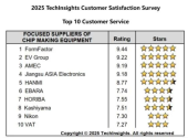
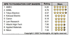
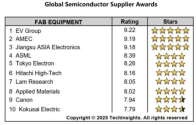
AMEC wins first place in two categories in TechInsights 2025 Semiconductor Supplier Awards Survey, with both its technical strength and service strength recognized.​


Shanghai, China, May 15, 2025 - Advanced Micro-Semiconductor Equipment (Shanghai) Co., Ltd. (hereinafter referred to as "AMEC", stock code: 688012) announced that it has won six awards in the 2025 Semiconductor Supplier Awards Survey organized by TechInsights, a global technology analysis and intellectual property service provider, including ranking first in the WFE to Foundation Chip Makers and Deposition Equipment lists.

In addition to winning the highest praise from customers in the above two lists, AMEC also won the following four awards:

  • Ranked third in the Global Semiconductor Supplier Awards – Top 10 Customer Service – Focused Suppliers of Chip Making Equipment

  • Ranked second in the Global Semiconductor Supplier Awards – Fab Equipment

  • Ranked third in the Global Semiconductor Supplier Awards – WFE to Specialty Chip Makers

  • Ranked first in the Global Semiconductor Supplier Awards – WFE to Foundation Chip Makers

1747685733338.png1747685774144.png
1747685797436.png

Please, Log in or Register to view URLs content!
 

tokenanalyst

Brigadier
Registered Member

Guangli Micro (Semitronix) Semiconductor Calibration Laboratory has passed CNAS accreditation.​


The calibration laboratory is equipped with world-leading advanced analytical instruments and calibration equipment, strictly implements the national "Metrology Law", "Quality Law" and other laws and regulations related to calibration, and has a complete set of scientific and standardized quality assurance systems and rules and regulations.

1747288703279.png


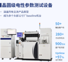
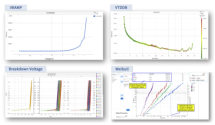
Guangliwei is committed to developing and providing technologically advanced and internationally competitive semiconductor parameter testing systems, horizontally expanding the categories of wafer-level reliability testing equipment to meet more diverse market demands .

Powerful machine performance
High precision: current test accuracy sub-pA, voltage test accuracy 100μV, capacitance test accuracy 10fF
Software and hardware collaboration: The "design and test collaboration" solution helps customers improve test productivity by dozens to thousands of times

Rich algorithm library
Covers WAT, WLR, Spice, Addressable circuit algorithms

Providing quality services
50+FAE team, with rich work experience, most of whom have a master's degree or above

Data analysis
Test data can be directly imported into Semitronix's own DE-G software and use the corresponding WAT/WLR data analysis module to improve user work efficiency.

1747691213684.png

1.WAT test
  • Accurate data: test data can match the baseline machine on the market​
  • High-efficiency production capacity: test speed is 1.4x-5x the market baseline​
  • Supports multiple types of wafer testing: covering LOGIC, CIS, DRAM, SRAM, FLASH, RO, BCD, etc.
    Rich algorithm library: support ID/VT/VTGM/IOFF/ISUB/BV/CAP/CV/IV/ICP, BETA/VBE/BVCEO/BVCBO/BVEBO, R2/RKLV/LK/CAP_METAL, IREAD/ISTANDBY/IDDQ/WM/SNM, ERASE/PROGRAM, IDDA/IDDQ/FREQ, etc.​
  • Software and algorithms are flexible and customizable​
2.WLR test
  • Accurate data: test data can match the baseline machine on the market​
  • Support HCI/ BTI/ VRAMP/ JRAMP/ VTDDB/ JTDDB/ EM/ PID/ SM/ ICP and other WLR tests​
  • Customized development can be performed according to test requirements, such as adding specific monitoring modes, outputting four-terminal Curve during VRAMP test, etc.​
  • Support intelligent parallel testing, greatly improving the testing speed​

1747691242403.png

At present, Guangli Micro can provide consulting, verification, testing and data analysis services related to semiconductor process reliability based on the industry-wide JEDEC or customer-customized standards . The test items include:
  • Gate oxide integrity (GOI Vramp/TDDB/Jramp)
  • Hot Carrier Injection (HCI)
  • Negative bias temperature instability (NBTI), etc.
  • It can also provide high voltage and parallel reliability testing to improve test efficiency and shorten the customer's process debugging cycle.
Please, Log in or Register to view URLs content!
 

tokenanalyst

Brigadier
Registered Member
HuaDa Empyrean takes the lead in formulating automotive-grade EDA group standards to help build China's industrial software standard system.

Recently, the China Electronics Standardization Association officially released two group standards, "Technical Requirements for Electronic Design Automation Tools for Automotive-Grade Universal Analog Integrated Circuits" (T/CESA 1384-2025) and "Technical Requirements for Electronic Design Automation Tools for Automotive-Grade Flat Panel Display Circuits" (T/CESA 1385-2025). These two standards were jointly developed by HuaDa JiuTian and many industry units to provide technical specifications for the development and application of automotive-grade EDA, fill the gaps in domestic standards in related fields, and accelerate the high-quality development of China's new energy vehicle industry.

The release of this group standard marks a key step in my country's standard construction in the field of automotive-grade EDA. As a leading domestic EDA company, HuaDa Empyrean has not only demonstrated its technological leadership by leading the formulation of standards, but also implemented the national strategy of "core technology autonomy" with practical actions, injecting new impetus into ensuring the security of the industrial chain and promoting industrial upgrading.

Please, Log in or Register to view URLs content!

Please, Log in or Register to view URLs content!
 

tokenanalyst

Brigadier
Registered Member

The hafnium-based ferroelectric FeRAM memory chip of the Institute of Microelectronics completed space experiments​

With the urgent demand for high-performance memory in aerospace equipment, traditional storage technology faces bottlenecks. The breakthrough of domestic FeRAM is expected to provide a new solution for the efficient and stable operation of aerospace equipment.
The team led by Researcher Luo Qing from the Institute of Microelectronics of the Chinese Academy of Sciences has developed the Mbit capacity radiation-resistant hafnium-based FeRAM memory chip MCF08M433. The chip uses doped HfO₂-based ferroelectric materials to solve the problems of poor compatibility of traditional ferroelectric materials with CMOS processes and difficulty in miniaturization, and achieves excellent radiation resistance through radiation-resistant reinforcement technology. The chip has the characteristics of high reliability, high speed, low power consumption, and strong radiation resistance. From January 2024 to date, the chip has completed space experiments to verify its reliable storage of programs, configuration parameters or computing data, proving its reliability in extreme environments and meeting the needs of the aerospace field.​

Please, Log in or Register to view URLs content!
 

tokenanalyst

Brigadier
Registered Member
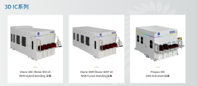
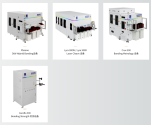
Piotech quietly launched their 3DIC series tools, standing for Three Dimensional Integrated Circuit, Include different types of Hybrid Bonders, Laser tools and Bonding Metrology Equipment.

1747692549943.png

1747692623912.png

TuoJing Technology debuts in Haining, Zhejiang, and continues to develop new 3D IC products​


Faced with the rapid development and technological iteration of 3D chips and advanced packaging , TuoJing Technology continues to develop new products and new processes to enhance the application coverage and mass production scale of thin film deposition and 3D IC equipment.

Tuojing Bond Technology is an important part of Tuojing Technology's industrial layout, focusing on advanced bonding technology and product research and development. In recent years, it has launched a number of advanced bonding products, fully demonstrating the company's technological innovation and achievement transformation capabilities, and its business scale continues to expand, steadily moving towards its vision of building a world-leading semiconductor equipment company.​

Please, Log in or Register to view URLs content!
 

tokenanalyst

Brigadier
Registered Member
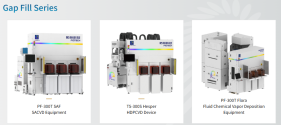
For the 3D Memory, 3D-NAND and the 3D IC looks like they also have the GapFill Series including a new tool the
PF-300T Flora Fluid Chemical Vapor Deposition Equipment.

1747693432483.png


The PF-300T Flora series is an ultra-high aspect ratio trench filling equipment independently developed by Tuojing. The equipment can achieve filling with an aspect ratio greater than 8:1 and is one of the important equipment for advanced process integrated circuit manufacturing. The equipment can deposit high-quality dielectric film materials such as SiO on the surface of the wafer. After UV or steam curing and oxidation processes, it can achieve the effect of completely filling the gap without leaving holes and gaps. It has now been industrialized.​
 
Top