SMIC is Shanghai, as they're the most prolific user of ASML machine, so that's their trump card. Huawei is Guangdong as they build a lot of technology cluster to support its technology development. So what about Beijing? will there be a champion to carry them? From what I'm seeing they will become a R&D center to support both of them.Not a 7nm Fab. From I heard, three 7nm or better Fabs. That makes sense because Ascend line , Kirin line should be separated. DUV and EUV line should be separated.
Guangdong would then overtake Shanghai in IC production
You are using an out of date browser. It may not display this or other websites correctly.
You should upgrade or use an alternative browser.
You should upgrade or use an alternative browser.
Chinese semiconductor thread II
- Thread starter vincent
- Start date
Beijing has SMIC beijing, Naura, RSlaser, Loongson. Shanghai has SMIC shangshai , Huahong, Unisoc, SMEE, Huawei Shanghai.SMIC is Shanghai, as they're the most prolific user of ASML machine, so that's their trump card. Huawei is Guangdong as they build a lot of technology cluster to support its technology development. So what about Beijing? will there be a champion to carry them? From what I'm seeing they will become a R&D center to support both of them.
Shenzhen has SMIC shenzhen, huawei and its fab and byd and its fab, cansemitech
Guangdong has lost of factories due to trade war since 2018 and tariff war currently.
So, local government have to plan for manufacturing that made stuffs that China market can use and not depending on other markets to absorb its traditional overcapacity.
Sicarrier duplicates everything Naura and SMEE do.
Shenzhen government invest alot in those area. I think they want to keep everything in that area and have new type of manufacturings.
It doesn't want to depend on other regions like beijing or shanghai.
"enriched water be kept inside"
The CloudMatrix Pod requires an incredible 6,912 400G LPO optical transceivers for networking,
Huawei compensated for its ascend chips against Nvidia by using superior networking technology
Huawei made their own optical transceiver in wuhan. It controls its cost unlike nvidia.
Huawei compensated for its ascend chips against Nvidia by using superior networking technology
Huawei made their own optical transceiver in wuhan. It controls its cost unlike nvidia.
Now they want to embed tracking and a kill switch into Nvidia chips.
Exclusive: US lawmaker targets Nvidia chip smuggling to China with new bill
U.S. Representative Bill Foster, a Democrat from Illinois who once worked as a particle physicist, said the technology to track chips after they are sold is readily available, with much of it already built in to Nvidia's chips. Independent technical experts interviewed by Reuters agreed.
Foster, who successfully designed multiple computer chips during his scientific career, plans to introduce in coming weeks a bill that would direct U.S. regulators to come up with rules in two key areas: Tracking chips to ensure they are where they are authorized to be under export control licenses, and preventing those chips from booting up if they are not properly licensed under export controls.
Foster's legislation would give the U.S. Department of Commerce six months to come up with regulations to require the technology.
The technology for verifying the location of chips would rely on the chips communicating with a secured computer server that would use the length of time it takes for the signal to reach the server to verify where chips are, a concept that relies on knowing that computer signals move at the speed of light.
proelite
Junior Member
Now they want to embed tracking and a kill switch into Nvidia chips.
This is going to cause more pain for legitimate customers than China.
The technology for verifying the location of chips would rely on the chips communicating with a secured computer server that would use the length of time it takes for the signal to reach the server to verify where chips are, a concept that relies on knowing that computer signals move at the speed of light.
Sooo if the WiFi is crap it will the server will think I am on the moon.
Huaxin Micro-Nano's 8-inch MEMS wafer production line project has completed the installation and commissioning of production equipment and is expected to be officially put into production in June
Recently, the 8-inch MEMS wafer production line project of Anhui Huaxin Micro-Nano Integrated Circuit Co., Ltd., with a total investment of 5.06 billion yuan, has made the latest progress. The project is currently in the process stringing stage of the main products and is expected to be completed by the end of June!
Public information shows that the 8-inch MEMS wafer production line invested and constructed by Anhui Huaxin Micro-Nano Integrated Circuit Co., Ltd. is located in Zone D of China Sensor Valley, with a construction investment of 5.06 billion yuan, a land area of about 154 acres, and a total construction area of 87,000 square meters. After the project is completed, the monthly production capacity will reach 30,000 pieces, and it is expected to become the largest MEMS wafer output production line in China. It will also be the first 8-inch piezoelectric MEMS mass production line in my country.
Huaxin Micro-Nano's 8-inch wafer production line project is mainly dedicated to the production and research and development of chips for sensors in the fields of industrial agriculture, medical vehicle electronics, and aerospace. At present, the project has completed the moving in and testing of all equipment, and the entire project is expected to be officially put into production in June this year.
It is understood that Anhui Huaxin Micro-Nano Integrated Circuit Co., Ltd. will be committed to continuing to lead MEMS wafer manufacturing technology, gradually forming an upstream and downstream industrial chain cluster, and leading and driving the domestic smart sensor industry cluster towards large-scale and high-end development.
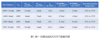
Basic Semiconductor Launches Next-Generation Silicon Carbide MOSFET
Recently, Basic Semiconductor officially launched a new generation of silicon carbide MOSFET series products, with further improved product performance and richer packaging forms. The first specifications include 1200V/13.5mΩ and 750V/10.5mΩ series for automotive main drive and other fields, 1200V/40mΩ series for photovoltaics, energy storage and other fields, and 650V/40mΩ series products for AI computing power supply, household storage inverter and other fields. Among them, the 650V/40mΩ series products achieve higher performance at low voltage levels by miniaturizing the cell spacing to 4.0μm. This series of new products will significantly improve the system efficiency and high temperature performance of terminal applications, reduce energy loss, and help the new energy field to achieve more efficient and economical power device solutions.


