You are using an out of date browser. It may not display this or other websites correctly.
You should upgrade or use an alternative browser.
You should upgrade or use an alternative browser.
Chinese semiconductor thread II
- Thread starter vincent
- Start date
What's the foundry for Cambricon chips?
I don't think you are wrong. These generation numbers are often used interchangeably and 920/910D could very well mean the same thing. I've definitely heard some industry people who would also refer to new Kunpeng chips as Kunpeng 930/940...960 instead of 920B/C...F, while the latter is definitely more commonly used. In fact, since Huawei has never officially named these chips, any naming can be correct as long as you are referring to the same thing.
Is the Ascend 910D different from Ascend 920 that is supposed to come in the next few months? Or did we just get the name wrong?
Chongqing Banan: The optoelectronic integrated high-end silicon-based wafer manufacturing center project capped
Guangyu Technology (Chongqing) Co., Ltd. held a capping ceremony for the "Photonics Integrated High-end Silicon-based Wafer Manufacturing Center Project" in Banan District, Chongqing. Banan District leaders, China Electronics System Engineering Third Construction Co., Ltd., representatives of many financial institutions and industry experts witnessed this important moment together.
The project is located in the Banan Digital Intelligence Industrial Park, with a total investment of 850 million yuan and a designed monthly production capacity of 3,500 high-end silicon-based wafers. It is expected to be put into production by the end of 2025. The parent company of Light Domain Technology is Xi'an Qixin Optoelectronics Technology Co., Ltd. ("Qixin Optoelectronics"), which focuses on the three major areas of "AI Intelligent Computing Center, Light Detection and Perception, and Light Computing" and is committed to creating a globally rare silicon photonics IDM model that integrates "material research and development, chip design, wafer flow, and packaging and testing". The capping of the project will inject strong momentum into the development of Qixin Optoelectronics and provide important support for the development of the domestic silicon photonics industry.
Since the official start of factory construction in October 2024, under the guarantee of the "special team promotion + full-cycle service" mechanism of the Banan District Committee and District Government, the project team has overcome the dual challenges of complex geological conditions and precise process requirements, shortening the construction period by 30% compared with the industry average, and completing the main structure construction in only 7 months, setting a new benchmark for the construction of silicon photonics wafer factories.
According to Huang Weihong, secretary of the board of directors of Qixin Optoelectronics, in the AI era, the huge market has driven a huge demand for intelligent computing power. Qixin Optoelectronics, which has been in this field for ten years, has ushered in a "boom" in business. The completion of this project will greatly alleviate the company's current production capacity bottleneck. At the same time, it is of great significance to shorten the new product development cycle, improve product profit margins, and accelerate the coordination of upstream and downstream industrial chains. After the project reaches full production, it is expected to produce 42,000 wafers annually, create 170 jobs, and drive the gathering of upstream and downstream supporting enterprises to form a tens of billions of industrial ecosystem.
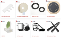
Applications of Advanced Ceramics For Semiconductor Industry
1. Ceramic substrate
Alumina, silicon nitride, aluminum nitride and silicon carbide ceramics have good thermal conductivity, high temperature and corrosion resistance, they can be used to produce substrates, for electronic components and integrated circuit;
2. Ceramic wafer tray
Alumina and silicon carbide ceramics have high temperature resistance, and wear resistance, they can be used to produce tray to carry wafer for various process, such as RTA(Rapid Thermal Annealing), PVD(Physical vapor Deposition), ICP(Inductively Coupled Plasma), CMP(chemical mechanical polish), to get good processing effect and high efficiency;
3. Ceramic vacuum chuck
Alumina and silicon carbide ceramics have good finish surface, with strong absorption force when pumping air is applied, also ceramic vacuum chuck have high temperature resistance, and widely used to absorb and transfer wafer during the production process;
4. Wafer boat and boat bracket
Silicon carbide and quartz have high temperature resistance and good wear resistance, also the density is low and weight is light, they are suitable to produce wafer boat and boat bracket, to carry wafer for diffusion and oxidation treatment in a diffusion furnace.
5. Diffusion furnace tube
Quartz tube has high temperature resistance and excellent thermal stability, it can be used as , for diffusion and oxidation process of semiconductor wafer wafer.


Professor Weijin Chen's research group at Sun Yat-sen University has made new progress in the research of ferroelectric multi-bit memory
Professor Chen Weijin's research group from the School of Materials Science and Engineering of Sun Yat-sen University and the Guangdong Provincial Key Laboratory of Magneto-Electrophysical Properties Analysis and Devices proposed a strategy to access multi-bit information using the multi-step polarization flipping characteristics of ferroelectric capacitors. Based on flip current sensing technology, this strategy only requires a single sense amplifier and a single operation to achieve accurate reading of different ferroelectric domain polarization states, and has an operating speed of nanoseconds, providing an effective way to improve the storage density of commercial ferroelectric memory products and realize storage-computing integrated operations.

Figure 1 Polarization reversal dynamics of ferroelectric devices with multi-domain structures
Studies have shown that when there are multiple types of ferroelectric domains, the polarization reversal of the ferroelectric film driven by an electric pulse can produce a transient reversal current response with multi-peak characteristics (Figure 1a), and is regulated by the rising edge of the electric pulse. The multi-domain structure of the ferroelectric film can be achieved by introducing the inhomogeneity of the crystal structure through defect engineering. Combining ultrafast pulse testing and polarization reversal dynamics simulation based on the nucleation-limited reversal model, the researchers pointed out that defects will cause the polarization reversal activation field of some ferroelectric domains to increase and the internal electric field distribution to broaden (Figure 1b).

Based on the multi-step polarization flipping characteristics of ferroelectric capacitors, the researchers demonstrated multi-bit binary information access and storage-computation-in-one operation schemes using a single-layer perceptron as an example at the circuit level (Figure 2a-c). The transistor-capacitor (1T-1C) circuit architecture and flip current sensing technology can convert the four ferroelectric domain polarization configurations into 2-bit binary digital signals (11), (10), (01) and (00), which is equivalent to doubling the storage density, as shown in Figure 2d. In addition, by combining with CMOS neuron circuits, storage-computation-in-one operation and pattern classification functions based on ferroelectric multi-bit memory can be realized (Figure 2e).
The achievement was published in the internationally renowned journal Advanced Functional Materials under the title of "Pulse-Modulated Polarization Switching Dynamics in Ferroelectric Thin Film for Circuit-Level Implementation of Multi-Bit FeRAM Cell". This work was independently completed by Sun Yat-sen University, with Tang Zhenxun, a doctoral student from the School of Physics, as the first author, and Professor Chen Weijin from the School of Materials and Guangdong Provincial Key Laboratory of Magnetoelectric Properties Analysis and Devices and Professor Zheng Yue from the School of Physics and Guangdong Provincial Key Laboratory of Magnetoelectric Properties Analysis and Devices as the corresponding authors. This research work was strongly supported by the National Natural Science Foundation of China, Guangdong Provincial Key Laboratory of Magnetoelectric Properties Analysis and Devices, Guangdong Provincial Basic Discipline Research Center for Magnetoelectric Properties, and the State Key Laboratory of Optoelectronic Materials and Technologies.
Another semiconductor project has been successfully capped
Wuxi Zhihe project is located in the west of Jinghui Road and the north of Xigang Road in Xishan District, Wuxi City, with a total construction area of about 19,052 square meters. The main products of this project include VOCs waste gas treatment equipment, stainless steel Teflon, stainless steel, galvanized air ducts and valves, and it is expected to create sales of 600 million yuan after reaching full production; the project belongs to the provincial advanced manufacturing high-end equipment cluster and will contribute to the high-quality development of Xibei Town.
According to the information, Zhihe Semiconductor Equipment (Jiangsu) Co., Ltd. was established on December 12, 2022. The legal representative is Guo Haifeng. The registered capital is 60 million yuan. The company's registered address is located at No. 12 Jingrui Road, Xibei Town, Xishan District, Wuxi City. The industry it belongs to is special equipment manufacturing. The business scope includes manufacturing of special equipment for semiconductor devices; sales of special equipment for semiconductor devices; manufacturing of semiconductor discrete devices; sales of semiconductor discrete devices; manufacturing of semiconductor lighting devices; sales of semiconductor lighting devices; sales of integrated circuit chips and products, etc.


