You are using an out of date browser. It may not display this or other websites correctly.
You should upgrade or use an alternative browser.
You should upgrade or use an alternative browser.
Chinese semiconductor thread II
- Thread starter vincent
- Start date
SMIC already has all the ASML lithography machines it needs for 70k wpm. The question is other toolsThe new Kirin 9020 is 140.5 mm2 -> 422 dies/wafer
Assuming a yield of 85% it means about 3.5M phones per 10K wafers, i.e. 40M phones/year, with 10K wpm of dedicated capacity.
We don't know current SMIC capacity at 7nm, it could be anything between 15K and 25K wpm or even 30Kwpm in the most optimistic case, but Kirin is only one of the many chips that SMIC has to fab at 7nm. With TSMC banned for advanced nodes, currently SMIC 7nm is a capacity bottleneck. Situation will improve when SMEE litho machines reach 7nm. The other Chinese SME players should be more or less already there.
I've had to resize your photo because it is huge. Please do this in the future or I'm going to have to ban you from this thread.
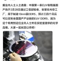
Also for this news, I just saw this as a social media posting, i wouldn't get too excited yet.
Sophgon built integrated compute platform using its 64-core RISC-V server CPU SG2044 that can do inference of DeepSeek R1 70B @ 11.8tps
Zhejiang and Garen Semi progress in Gallium Oxide ingot, wafer and equipment.
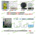
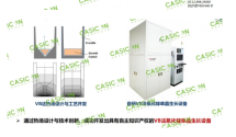
Professor of Zhejiang University and chairman of Hangzhou Gallium Semiconductor Co., Ltd., delivered a keynote speech on "Progress in Large-Size High-Quality Gallium Oxide Single Crystal Materials" at the "Sub-Forum 2: Gallium Nitride and Other Power Semiconductor Technologies and Applications". He shared the latest progress in gallium oxide single crystal growth technology, Czochralski, casting and VB single crystal growth research and development. The report pointed out that there are many methods for growing gallium oxide crystals, and casting and VB methods have shown great potential for large-scale industrialization in terms of size, cost, quality and many other aspects.
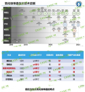
The casting method and other technologies developed by its team have successfully achieved the growth of large-size (6-inch) gallium oxide crystals with multiple crystal orientations and different doping, which can meet various epitaxy and device requirements. According to estimates, after mass production of its existing technology, the cost of 6-inch substrates can be reduced to less than 2,000 yuan, and further cost reduction will be completed within 2 to 3 years, providing the industry with high-quality, low-cost substrates. High-quality, low-cost substrates can assist peers in overcoming some key problems, such as defect behavior, p-type doping, and large-area, high-current devices. The industrialization process of gallium oxide will gradually accelerate, and the combination of substrates, epitaxy, devices, and applications should be closer to achieve transcendence.
DRAM before logic? Doubtful.
Nanxin Technology changes its fundraising and investment project and plans to invest 1.443 billion yuan to build a chip testing industrial park
Nanxin Technology issued an announcement stating that the company's original fundraising project was a test center construction project, and it is now planned to be changed to a chip testing industrial park construction project. The total investment in the project is 1.443 billion yuan, and it will be constructed in two phases, with an investment of 713 million yuan in the first phase and 730 million yuan in the second phase. The company will use the remaining funds raised from the original fundraising project and its interest of 282 million yuan, as well as the remaining over-raised funds and its interest of 312 million yuan, for a total of 595 million yuan in raised funds for the first phase of this project.
Nanxin Technology issued an announcement stating that the company's original fundraising project was a test center construction project, and it is now planned to be changed to a chip testing industrial park construction project. The total investment in the project is 1.443 billion yuan, and it will be constructed in two phases, with an investment of 713 million yuan in the first phase and 730 million yuan in the second phase. The company will use the remaining funds raised from the original fundraising project and its interest of 282 million yuan, as well as the remaining over-raised funds and its interest of 312 million yuan, for a total of 595 million yuan in raised funds for the first phase of this project.
Baoxin Technology acquires 40% equity of Yingsu Integration for RMB 320 million
On the evening of March 3, Baoxin Technology announced that the company acquired 40% of the equity of Jiangsu Yingsu Integrated Equipment Co., Ltd. (referred to as "Yingsu Integration", "Target Company" or "Target Company") in cash through its consolidated subsidiary Zhejiang Yingsu Integrated Equipment Manufacturing Co., Ltd. (referred to as "Zhejiang Yingsu") After the completion of this transaction, Zhejiang Yingsu will become the controlling shareholder of Yingsu Integration. After negotiation, it was determined that the transaction value of Yingsu Integration's equity transfer was based on an overall valuation of 800 million yuan, and the corresponding transaction price of 40% equity was 320 million yuan.
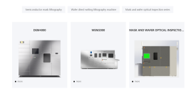
Data shows that Yingsu Integration was jointly initiated by my country's professional R&D and manufacturing team in the field of lithography and the Institute of Microelectronics of the Chinese Academy of Sciences. It is mainly engaged in the research and development, manufacturing and sales of high-end microelectronic equipment with laser direct writing lithography technology as the core. Its products include laser direct imaging (LDI) equipment for PCBs and laser direct writing lithography equipment for semiconductor masks. Previously, there were 139 valid patents, including 47 invention patents, 84 utility model patents, and 8 design patents. Yingsu Integration is also a national high-tech enterprise, a Chinese industry-university-research cooperation innovation demonstration enterprise, a Xuzhou patent little giant enterprise, a member unit of the National Integrated Circuit Packaging and Testing Industry Chain Technology Innovation Alliance, and a Jiangsu Province Specialized and New Little Giant Enterprise.
Baoxin Technology stated that this acquisition was based on the company's strategic layout. Yingsu Integration can complement the company's advantages in sales, management, talents, etc., which will help the company build a confident system product, thereby enhancing the company's sustainable development capabilities and core competitiveness, effectively enhancing the company's profitability, fully protecting the interests of investors, and expanding new carriers and platforms for the company's business development. It will continue to develop, invest, and acquire related assets, achieve controlling stakes in high-quality projects and inject them into listed companies, invest in important semiconductor companies, develop and support China's semiconductor industry, and achieve corporate value-added capital investment returns.
China's supply chain reshapes the global traction inverter industry landscape, with Huawei becoming one of the top five suppliers
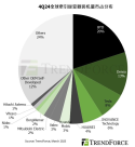
According to the latest research by market research firm TrendForce on March 4, the total installed capacity of electric vehicle traction inverters in the world will reach 8.67 million units in the fourth quarter of 2024, a 26% increase from the previous quarter. Among them, the strong demand in the Chinese mainland and European markets has become the main driving force for the growth of the market, driving the installed capacity of pure electric vehicles (BEV) and plug-in hybrid electric vehicles (PHEV) to grow by 28% from the previous quarter, and pushing Huawei into the top five global suppliers.
TrendForce indicates that the global traction inverter market will have installed capacity of 27.21 million units in 2024. Among them, SiC (silicon carbide) inverters benefited from the adoption of Tesla and Chinese car manufacturers, with the penetration rate reaching 16% in the fourth quarter, the highest of the year, which is a positive signal for the highly competitive power semiconductor industry.
