You are using an out of date browser. It may not display this or other websites correctly.
You should upgrade or use an alternative browser.
You should upgrade or use an alternative browser.
Chinese semiconductor thread II
- Thread starter vincent
- Start date
Haiguang Intelligent Technology innovative design in large-scale high-power MPCVD equipment
Diamond is recognized as the "ultimate choice" for the next generation of semiconductor materials due to its ultra-wide bandgap (5.5 eV), ultra-high thermal conductivity (2000 W/m・K), high breakdown field strength (10 MV/cm) and excellent chemical stability, especially in the field of high-frequency, high-temperature and high-power electronic devices. However, the preparation of semiconductor-grade diamond has long been limited by large-size single crystal growth technology, and the innovative design of microwave plasma chemical vapor deposition (MPCVD) equipment has become the core path to break through this bottleneck.

Power improvement and structural optimization
The 15kW MPCVD equipment launched by Haiguang Intelligent Technology stabilizes the plasma fireball coverage area at more than 4 inches by improving the microwave transmission system and heat dissipation design, achieving stable growth of single-crystal diamond with a diameter of 100 mm, with a growth rate of 9-12 microns/hour, and the temperature difference between the center and the edge is controlled within a very small range. The equipment uses a metal sealing ring to replace the traditional rubber ring, combined with a copper substrate table to improve thermal conductivity, effectively solving the long-standing plasma instability problem of domestic equipment.
Breakthroughs in Intelligence and Automation
The fully intelligent MPCVD equipment developed by Carbon Equation realizes one-button start, multi-parameter real-time monitoring and automatic adjustment functions, and dynamically optimizes gas flow, microwave power and temperature curve through AI algorithms, significantly reducing the need for manual intervention. The equipment can centrally manage dozens of devices through a central control system, shortening the fault response time to seconds, and supporting remote operation and maintenance and cloud storage of process parameters.
Domestic Substitution Process
The cost of MPCVD equipment independently developed by Ningbo Institute of Materials Technology and Engineering, Chinese Academy of Sciences is only 1/10 of that of imported equipment. Through multiple iterations of optimization, it has built the world's largest CVD single crystal diamond production line (more than 1,000 equipment), achieving mass production of 42mm×42mm single crystal diamonds, with quality benchmarking the international advanced level. The Z-axis automatic lifting platform developed by it has obtained a national patent, which optimizes the temperature field distribution by accurately adjusting the substrate height, reducing the thermal resistance of the diamond-substrate interface by 30%.
Fuzhou University and others make breakthrough in Micro LED mass transfer technology
Fuzhou University, in collaboration with Chalmers University of Technology, has made a significant breakthrough in Micro LED mass transfer technology. The team developed a novel laser-induced transfer method that achieves ultra-high yield (100%) without residual polymer, addressing key challenges in large-scale production. By optimizing laser energy (1200–1500 mJ/cm²) and spot size (30×38 microns), the process ensures precise chip alignment, avoids surface damage, and maintains stability. Traditional methods like electrostatic adsorption or micro-stamping face limitations such as charge accumulation or misalignment, but this new approach overcomes these issues with superior flexibility and accuracy. The research also resolved problems caused by polymer-based substrates (e.g., PDMS) through a mathematical model linking chip sinking depth to optimal laser energy, enabling precise, residue-free transfers.
This scalable technology works across various Micro LED chip sizes, paving the way for applications in AR/VR, wearables, and smart displays. Fuzhou University, home to the National New Display Technology Innovation Center, has long led Micro LED research, collaborating with industry partners like Hymxing and academic institutions to advance the field. Future goals include expanding the technology to full-color Micro LEDs, flexible displays, and micro-projection, solidifying its role in next-generation display innovations.
Focusing on compound semiconductors, 48th Institute (CETC) won an order for MOCVD equipment worth over 100 million yuan.
Recently, the 48th Institute of China Electronics Technology Group Corporation (hereinafter referred to as "Institute 48") signed an MOCVD equipment order worth over 100 million yuan with a leading domestic enterprise, and signed a large-scale MOCVD supply strategic cooperation agreement with a leading domestic gallium arsenide enterprise.
It is reported that the MOCVD equipment developed by the 48th Institute is a key equipment dedicated to the epitaxial growth of III-V compound semiconductor materials. The equipment is based on the arsenic/phosphorus material system and can efficiently prepare materials such as gallium arsenide and indium phosphide.

At the same time, the equipment is suitable for optoelectronic lasers, radio frequency devices, space solar cells and other fields, providing a core material preparation platform for emerging technologies such as 5G communications, artificial intelligence and autonomous driving. The equipment integrates advanced technologies such as online monitoring and fully automatic transmission, and has reached industry-leading levels in key indicators such as material uniformity, interface steepness and doping accuracy.
According to the data, the 48th Institute is one of the leading enterprises in the field of compound semiconductor epitaxy equipment in China, and has successfully launched a series of equipment such as SiC epitaxy furnaces, MBE equipment and MOCVD. The latest breakthrough in MOCVD equipment will further expand the business scope of the 48th Institute in the semiconductor field and better assist the construction of the national semiconductor equipment industry cluster.
Using AI for SME monitoring and fault detection.
EqFuse device intelligence series, let each device have a smart brain that can "talk, think and optimize"
The EqFuse equipment intelligence series is an OEM intelligent solution built by Zhixian Future specifically for semiconductor equipment manufacturers . The solution embodies Zhixian Future's more than 20 years of semiconductor industry software accumulation, and deeply integrates engineering intelligent product functions such as chamber matching (Chamber Matching), fault monitoring and classification (FDC) and recipe management system (RMS) . It also combines the best algorithms, big data, big language models and AI technology to configure the equipment with"can talk, think and optimize", realizeintelligent fault diagnosis and prediction, self-tuning and intelligent manufacturing, and maximize equipment value and production efficiency.

- Chamber Matching
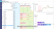
Chamber Matching is the core function of EqFuse, which can help equipment engineers quickly analyze the gap between equipment/chambers and save machine adjustment time.
Taking thin film deposition as an example, the number of chip processing layers often reaches hundreds. Due to differences in equipment and chambers, it is impossible to ensure the consistency of process performance. The traditional method relies on engineers' experience and manual comparative analysis to find the root cause of the problem, which usually takes hours or even days.
The device has built-in Chamber Matching function, which can realize fully automated intelligent analysis, greatly shorten the analysis time, and redefine the intelligent device solution:
- Parallel analysis of chambers is not limited in number .
- Automatically identify and match the "best chamber" based on the successfully verified optimal algorithm and perform difference comparison
- Full Trace full parameter comparison analysis
- Accurately locate mismatch parameters and specific mismatch steps
- One-click FDC verification: Jump to the FDC traceability details analysis page with one click to verify the matching results of mismatch parameters.


- FDC fault monitoring and classification - fault warning sentinel
Real-time monitoring of the operating status of equipment during the production process replaces post-production detection, captures anomalies in advance, and accurately locates the source of the problem, providing strong support for troubleshooting and equipment optimization.
- RMS process formula management——formula safety fortress
Through central control, the formula and equipment are seamlessly connected, the production process is optimized, management efficiency is greatly improved, and intelligent and efficient formula management is achieved.
- AI+RCA fault root cause analysis——fault location radar
Fusion Intelligence presents the future industry vertical big model "Lingxi", intelligently diagnoses equipment causes. Comprehensively analyzes multiple data such as recipes/equipment constants/equipment change records, so as to quickly and accurately locate the root cause of equipment problems.
- AI Assistant: A know-it-all for devices, who understands them better than device engineers
The AI Assistant knowledge base service is built by integrating more than 200 industry scenarios of Zhixian Future , 40TB of semiconductor industry data, professional paper knowledge, engineer work orders/reports , etc., which can realize troubleshooting, rapid recall and display of fault cases, visual source location, automatic retrieval of equipment parameters, equipment fault troubleshooting and maintenance plan recommendations, etc., which greatly improves the troubleshooting efficiency and "understands" the equipment better than equipment engineers.
- AI+EHM health prediction management
Combining historical data with cloud computing capabilities, prediction algorithms, large language models and other technical means, early abnormal signals in abnormal modes can be identified, faults can be accurately predicted in advance, and detailed maintenance plans can be generated. This measure has changed the previous situation of heavy reliance on the experience of veterans and lack of systematic and scientific prediction methods. From "passive processing" to "autonomous defense", it has greatly improved the ability to prevent and handle equipment failures and reduced production interruptions caused by equipment failures.
Tin droplet target generation method and system
Abstract
The invention relates to the technical field of EUV light sources, and discloses a tin droplet target generation method and system. The tin droplet target generating system comprises two generating devices for generating tin droplets and a signal generating device for regulating and controlling the division of the tin droplets, and a tin droplet fog spot is generated by colliding the two tin droplets, wherein the droplet diameter in the fog spot is far smaller than that of the droplet for collision. The tin liquid drop fog spots generated in the mode replace the existing fog spots formed after the prepulse bombardment, and the structure of the EUV light source is simplified. The shape and the size of the fog spots can be adjusted through collision angles, so that the fog spots of the strip-shaped liquid drops can be conveniently generated and matched with the light spots of the slat lasers. The strip laser with strip light spots can be used for bombarding strip low-density tin droplet fog spot targets generated by droplet collision, and plasma containing EUV light can be generated. The technology provides a new technical scheme for the EUV light source, so that a droplet target can be more conveniently and stably generated, and pre-pulse can be avoided during targeting.
Fudan University receives 3.5 million RMB technology service contract from Fudan Microelectronics to develop ultra-large-scale FPGA technology
Fudan Microelectronics announced that it plans to sign a technical service contract with Fudan University, entrusting the university with the research and development of ultra-large-scale FPGA layout and routing technology and the provision of corresponding technical support. The contract value is RMB 3.5 million. The transaction is classified as receiving related-party services.
The contract will take effect on July 28, 2025, and end on December 31, 2026. The intellectual property rights of the research and development will belong to the company.
Fudan Microelectronics stated that, with Fudan University's State Key Laboratory of Integrated Chips and Systems and School of Microelectronics, equipped with advanced equipment and employing a large number of cutting-edge professionals with extensive knowledge and experience in microelectronics research and development, the company and Fudan University are jointly promoting industry-university-research collaboration, which will benefit the company's operations.
It further stated that the company maintains a stable cooperative relationship with Fudan University, and this related transaction will not have an adverse impact on the company's independence, and the company's main business will not become dependent on related parties due to such transactions.
Qinghe wafer bonding technology breaks through the bottleneck of GeOI industrialization: heat dissipation efficiency increased by 40% and bonding area increased to more than 95%!
Germanium has a high refractive index. When light enters germanium from a medium, it is deflected at a large angle. This property gives germanium a powerful ability to manipulate light and accurately change the propagation path of light, providing rich possibilities for the design and application of optical devices.
As a key solution for next-generation semiconductor materials, GeOI (Germanium on Insulator) substrate technology, with its unique properties, offers significant advantages in high-frequency electronics, optoelectronic integration, and quantum computing. By integrating a thin germanium film onto an insulating layer, this technology combines the high carrier mobility of germanium with the proven properties of silicon-based processes. Globally, GeOI technology is currently at a critical stage of transition from laboratory research and development to industrialization.
Key technological breakthroughs
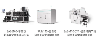
To address the above challenges, Qinghe Jingyuan's SAB61 ultra-high vacuum room temperature bonding equipment provides innovative solutions:

In terms of thermal management
The device utilizes room-temperature bonding technology, achieving atomic-level bonding through plasma activation in an ultra-high vacuum (10⁻⁶Pa) . This process completely avoids the thermal stress associated with traditional high-temperature bonding, and actual measurements show a 40% improvement in device heat dissipation efficiency.
In terms of bond strength
The natural oxide layer is removed through cleaning process or plasma activation to improve the cleanliness of the bonding surface and enhance the bonding interface strength.
In terms of mass production costs
The equipment supports mixed-line production of 2- to 12-inch wafers and integrates an H-cut recycling module . This design increases germanium material utilization by over 80% , reducing the production cost of a single 8-inch GeOI substrate from $200 to $75.

Feidong large-size semiconductor-grade monocrystalline silicon rod project will be put into production
Reporters from the Feidong County High-End Equipment Intelligent Manufacturing Industrial Park learned that the large-scale Semiconductor-grade monocrystalline silicon ingot production project of Anhui Lianxiao Technology Co., Ltd. (hereinafter referred to as "Lianxiao Technology"), a company within the park, is entering the final stages of equipment commissioning and will soon transition to hot commissioning, with official production expected to begin in October . This project, with a total investment of 1.4 billion yuan, will not only provide key support for the improvement of the semiconductor industry chain in Feidong and the entire province, but also has the potential to address the country's dependence on imports for large-scale monocrystalline silicon.
"From acquiring land to building a factory, we have 'escorts' all the way!" The person in charge of Lianxiao Technology said that during the promotion of the project, local relevant departments and the local government followed up throughout the process, actively connected and provided efficient services in land planning, construction approval and other links, providing all-round element guarantees for the rapid implementation of the project.Today, four standardized factory buildings, a comprehensive building and employee dormitories have been completed in the 54,000- square-meter factory area . After production, they will provide 200 jobs and the annual output value is expected to exceed 500 million yuan.
As a national high-tech enterprise, Lianxiao Technology is deeply engaged in the research and development and manufacturing of large-size monocrystalline silicon of 12~19 inches. Its products can meet diverse needs such as high, medium and low resistance.


