Chinese semiconductor thread II

tokenanalyst

Brigadier
Registered Member

Comparative study of single event upset susceptibility in the Complementary FET (CFET) and FinFET based 6T-SRAM​

Abstract​

The Complementary FET (CFET) architecture offers a more promising solution for achieving higher transistor density in sub-3 nm technology nodes. In this study, we use 3D TCAD simulations to conduct Monte Carlo based single-particle incidence analysis on FinFET and four types of CFET 6-Transistor (6T) Static Random Access Memory (SRAM). We identify the linear energy transfer (LET) thresholds for the five SRAM structures and analyze the causes of Single Event Upset (SEU) in three sensitive areas. Simulation results indicate that the SEU LET threshold of the CFET SRAM in the Fin-On-GAA-Fin (FOGF) structure is higher than that of the Fin-On-Trapezoidal-Fin (FOTF) structure. This is because both the upper and lower layers of the CFET SRAM in the FOGF structure use the GAA structure to isolate from the substrate, making it more difficult to trigger the bipolar amplification effect. The CFET SRAM using the Staggered FOGF structure demonstrates the best radiation resistance when the LET is below 0.3 pC/μm, due to the more dispersed distribution of sensitive areas and the isolation of the lower PMOS from the substrate. We also calculate the SEU cross-sections of the five SRAMs under different LETs. Showing that CFET SRAM consistently exhibits better radiation resistance compared to FinFET SRAM. These findings suggest that advanced CFET technology could be effectively applied to the design of radiation-hardened SRAM.​


Please, Log in or Register to view URLs content!
 

tokenanalyst

Brigadier
Registered Member

MiG Lab completes strategic financing of nearly 100 million yuan to accelerate the creation of a global benchmark for semiconductor testing​


MiG Lab recently announced the completion of a strategic financing of nearly 100 million yuan, committed to accelerating the breakthrough of semiconductor testing technology barriers, promoting the localization process, and leading a new paradigm in scientific research testing services.

Accelerate the creation of a global benchmark for semiconductor testing

Recently, Beijing Jurui Zhongbang Technology Co., Ltd. (brand: MiG Lab), a leading new material and semiconductor research and testing platform in China, officially announced the completion of nearly 100 million yuan in strategic financing. This round of financing was jointly invested by Bazhou Optical Valley Industrial Development Fund managed by China Electronics Zero Capital, Chengdu Wutong Zhongge Equity Investment Fund managed by Chengdu Science and Technology Venture Capital, and Beijing Huairou Science City Science and Technology Innovation Investment Fund managed by Shunxi Fund. The funds will be used to enhance core technical capabilities, improve the layout of the national laboratory network, deepen the international SEMI certification system, and promote the localization of semiconductor testing equipment.

Deeply cultivate "hard technology" and build semiconductor testing technology barriers

MiG Lab was established in 2016 and was born out of the Institute of Semiconductors of the Chinese Academy of Sciences. With the mission of "activating global scientific research resources and revitalizing Chinese science and technology", it focuses on high-end testing services in the fields of semiconductors, new materials, integrated circuits, aerospace, etc. As the only platform-based enterprise in the country that integrates scientific research resources through market-oriented operations, MiG Lab has built a three-in-one service network of "centralized shared laboratories + distributed shared laboratories + open cloud platforms", covering core industrial areas such as the Beijing-Tianjin-Hebei region, the Yangtze River Delta, the Guangdong-Hong Kong-Macao Greater Bay Area and the Western Science City, and has integrated laboratory resources from more than 550 universities and institutes to serve well-known domestic companies and more than 2,000 high-tech companies.

The company has 16 industry qualifications including SEMI international certification and CNAS laboratory accreditation. The core technical team comes from the Chinese Academy of Sciences, and the chief scientist, Academician Wang Zhanguo, leads a think tank of more than 550 experts to provide support. Its 10 product line technologies such as electron microscope detection, failure analysis, and material analysis have been verified by leading companies, and its domestic market share is leading, especially in the field of SEMI certification, serving more than 150 leading semiconductor equipment manufacturers, helping domestic equipment enter the international supply chain.


Please, Log in or Register to view URLs content!
 

tphuang

General
Staff member
Super Moderator
VIP Professional
Registered Member
btw, if you are going to make a short snide remark on the BIS/Huawei thing, it will be deleted. Please provide quality feedback.
 

tokenanalyst

Brigadier
Registered Member
The issue is that these are unenforceable rules for US politicians to feel good.

- How many US executives are prison?
- How many Companies have been fined?
- How many extraditions?

Very close to zero, the US doesn't have the capabilities to enforce these rules, not even inside the US. I understand the people in the US want to feel good in their hegemonic illusion that the US is capable of everything. The reality is prove them wrong again and again.

Their best chance is to relax the diffusion rule for companies who prefer to buy Nvidia GPUs but that will open for them another can of worms.
 
Last edited:

tokenanalyst

Brigadier
Registered Member

Jingsheng Electromechanical successfully developed a 12-inch conductive SiC crystal​


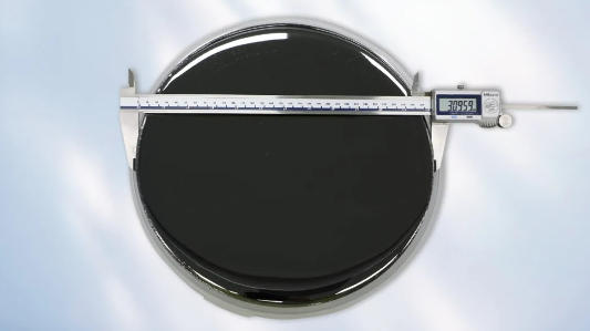
Zhejiang Jingrui Electronic Materials Co., Ltd. (hereinafter referred to as "Zhejiang Jingrui SuperSiC"), a subsidiary of a subsidiary of Jingsheng Electromechanical, , has achieved a breakthrough in the growth technology of 12-inch conductive silicon carbide (SiC) single crystals. The first 12-inch SiC crystal was successfully produced - the crystal diameter reached 309mm and the quality was intact .

MBXY-CR-33074d4a866c03fd32f8f47b2d2626ad.png

The first 12-inch conductive silicon carbide (SiC) single crystal


Zhejiang Jingrui SuperSiC, based on its independently developed SiC single crystal growth furnace and continuously iteratively upgraded 8-12 inch crystal growth process, has, after years of technical research and development, innovated the crystal growth temperature field design and gas phase raw material distribution process, and successfully overcome the core problems of uneven temperature field and crystal cracking in the growth of 12-inch SiC crystals, achieving an important breakthrough in the growth of 12-inch ultra-large size crystals .

The successful breakthrough of Jingsheng Electromechanical's 12-inch conductive SiC crystal not only marks that Jingsheng Electromechanical has achieved independent control of 6-12 inch full-size crystal growth technology in the SiC field, but also provides strong technical support for the independent development of my country's SiC industry chain.

Please, Log in or Register to view URLs content!
 

tokenanalyst

Brigadier
Registered Member

Key technology for large-size diamonds! West Lake Instruments achieves breakthroughs in laser stripping efficiency and loss!​


Westlake Instruments officially released the large-size single-crystal diamond high-efficiency laser lift-off technology at the Second International Conference on Optoelectronic Integration Technology (COINT 2025) , achieving breakthrough progress in core indicators such as loss control, processing efficiency, and process stability, providing key technical support for the industrialization of diamond semiconductors.

1747171969755.png1747172382325.png

Diamond, known as the "ultimate semiconductor material", has material properties such as ultra-wide bandgap, high thermal conductivity, high breakdown field strength, high carrier saturation drift velocity, and is also radiation-resistant.

Diamond's many excellent properties make it have broad application prospects in heat sinks, semiconductors, optics and other fields (see the end of the article for details), but there are still many problems to be solved in the industrialization of high-quality semiconductor diamond materials. Diamond is a superhard material. To achieve the cutting and successful stripping of large-sized diamonds, the use of traditional laser cutting technology is not only costly but also inefficient.

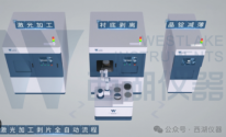
In response to this pain point, Westlake Instruments has developed a set of practical solutions for the high-efficiency and low-loss production of large-size diamond substrates, which greatly reduces material loss and shortens processing time . Taking the processing of 1-inch diamond as an example, the comparison between this technical solution and traditional laser cutting technology is as follows:

Diamond application prospects:

Heat sink field

The thermal application range of CVD diamond is very broad, such as making heat sinks for high-power density circuit components such as array devices, microwave tubes, laser diodes, and high-power integrated circuits, thereby improving the working efficiency and power life of the device.

Semiconductor field

One of the applications of diamond semiconductor devices is electron tubes. The biggest benefit of replacing these electron tubes is that the devices become smaller and lighter, and the operating voltage and other performance can be greatly improved. For example, some novel devices can be reflected by the unique properties of diamond in design and processing. Its emergence can not only have an impact on wide bandgap devices, but also shake the position of traveling wave tubes (TWT) in the RF power supply market.

Optical field

Diamond can be used as a protective film for optical lenses, but currently, due to the high cost of preparing diamond films, it is only used in the field of military optics. In addition to being used in the military field, optical-grade diamond films can also be used for window materials (such as X-ray windows, infrared windows, etc.) and protective coatings for optical discs, lenses, windows, ultraviolet lasers, millimeter-wave antenna covers, etc.

Please, Log in or Register to view URLs content!

Please, Log in or Register to view URLs content!


tphuang

General
Staff member
Super Moderator
VIP Professional
Registered Member
The issue is that these are unenforceable rules for US politicians to feel good.

- How many US executives are prison?
- How many Companies have been fined?
- How many extraditions?

Very close to zero, the US doesn't have the capabilities to enforce these rules, not even inside the US. I understand the people in the US want to feel good in their hegemonic illusion that the US is capable of everything. The reality is prove them wrong again and again.

Their best chance is to relax the diffusion rule for companies who prefer to buy Nvidia GPUs but that will open for them another can of worms.
that's fine, but if you are going to post, put more than just 1 line and a mocking photo. That's low quality posting.

You've been on this forum long enough to know that is low quality posting.
 
Top