You are using an out of date browser. It may not display this or other websites correctly.
You should upgrade or use an alternative browser.
You should upgrade or use an alternative browser.
Chinese semiconductor thread II
- Thread starter vincent
- Start date
A new breakthrough in domestic EDA, Innova launches RTL power consumption optimization tool!
Enfortius (Chengdu) Electronic Technology Co., Ltd. has launched EnFortius® RTL Power Explorer (ERPE), an early RTL-level power optimization tool for chip design. This tool can efficiently and comprehensively analyze and explore power optimization opportunities in the RTL design stage, helping designers to minimize chip power consumption. The ERPE product will also be unveiled at IIC Shanghai on the 27th and 28th of this month.
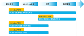
Enfortius (Chengdu) Electronic Technology Co., Ltd. has launched EnFortius® RTL Power Explorer (ERPE), an early RTL-level power optimization tool for chip design. This tool can efficiently and comprehensively analyze and explore power optimization opportunities in the RTL design stage, helping designers to minimize chip power consumption. The ERPE product will also be unveiled at IIC Shanghai on the 27th and 28th of this month.

Huafeng Measurement & Control: Good orders in hand, expected to continue growth in 2025
Huafeng Testing & Control said in an institutional survey that the company's current orders are in good condition and are expected to continue to grow throughout 2025. The semiconductor industry will recover after a cyclical adjustment in 2024. With the expected recovery in demand in the automotive, industrial and consumer electronics terminal markets, the semiconductor equipment market is expected to continue to benefit in 2025.
Regarding the decline in gross profit margin in the fourth quarter of 2024, the company's gross profit margin in the fourth quarter of 2024 was 66.18%, a year-on-year decrease of 4.3%. The company explained that this was mainly due to the adjustment of the new accounting standards, which led to the concentration of data in the fourth quarter, but the full-year gross profit margin increased by 2 percentage points year-on-year.
In terms of new product layout, the high-end test equipment STS8600 is currently in the customer verification stage. The company is continuously polishing product performance and plans to cover more market areas by launching new boards and cards, and to improve customer recognition with the help of innovative technologies, with the goal of building it into an industry-leading semiconductor test platform. At the same time, the company has established mature solutions in the field of KGD (known good product) testing, and has deepened cooperation with domestic and foreign customers, and its market share is expected to increase steadily in the future.
In addition, the progress of the company's self-developed ASIC chip project has attracted attention. The project aims to promote the high-end development of test equipment and solve the problem of independent control of chips through cooperation with the industry chain. The company said that due to the influence of the external environment, the self-development plan was launched ahead of schedule, and in the future it will rely on customized chip technology to enhance equipment performance and consolidate industry competitiveness.
Weice Technology plans to invest 1.3 billion yuan to build the second phase of the Nanjing test project
Weice Technology issued an evening announcement stating that in order to increase the proportion of high-end chip testing business and testing service level and expand market share, the company's wholly-owned subsidiary Nanjing Weice Semiconductor Technology Co., Ltd. plans to use no more than 1.3 billion yuan to invest in the Weice integrated circuit chip wafer-level and finished product testing base project (Phase II).
The announcement stated that this project is actually an expansion project for integrated circuit chip wafer-level testing and finished product testing. After the project is completed, the company's production capacity, especially the "high-end chip testing" and "high-reliability chip testing" capacity will be further improved. The construction of this project is in line with the industry development trend and strategic development direction, which is conducive to the company's continued growth in performance and further consolidation of its industry position.
Major progress in diamond semiconductors in China
2-inch heteroepitaxial single crystal diamond has achieved domestic mass production
Professor Wang Hongxing's team at Xi'an Jiaotong University has successfully achieved mass production of 2-inch heteroepitaxial single-crystal diamond self-supporting substrates through the independently developed MPCVD (microwave plasma chemical vapor deposition) technology.
Breakthrough in (111) crystal face diamond epitaxy technology
Wang Hongxing's team further achieved epitaxial growth of 1-inch (111) oriented single crystal diamond on Ir (111)/sapphire heterogeneous substrates. The crystal quality was verified by SEM, XRD and other characterizations, laying the foundation for the research and development of diamond-based GaN power devices, which can promote the performance of RF devices to improve by more than 40% in the future.
Commercialization of polycrystalline diamond is accelerating
Henan Huanghe Cyclone Company announced that it has successfully developed a CVD polycrystalline diamond heat sink. The product has a diameter of 2 inches and a thickness range of 0.3 to 1 mm. Huanghe Cyclone and Xiamen University Sa Bendong Micron and Nano Science and Technology Research Institute have established a joint integrated circuit thermal control laboratory to carry out innovative research on integrated heat dissipation applications based on diamond materials to solve the chip heat dissipation problems in the fields of 5G/6G, AI and phased array radar.
Flexible ultra-thin diamond film technology breakthrough
Peking University, in collaboration with Southern University of Science and Technology and the University of Hong Kong, has successfully developed large-area (2-inch wafer), ultra-thin (sub-micron thickness), ultra-flat (surface roughness less than nanometers), and ultra-flexible (360° bendable) diamond films. This innovative achievement is not only a milestone in the field of materials science, but also paves the way for the commercial application of diamond films.
Recently, the team of Professor David Di and Professor Baodan Zhao from Zhejiang University published a paper titled "Downscaling micro- and nano-perovskite LEDs" in Nature.
The team created micro- and nano-perovskite LEDs (micro- and nano-PeLEDs) with pixel sizes ranging from hundreds of microns to 90 nanometers , the smallest LED pixels disclosed to date. At the same time, they created an LED pixel array with an ultra-high resolution of 127,000 PPI , setting a record for the highest resolution of all types of LED arrays
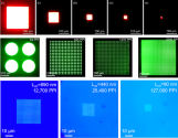
The paper states that the current manufacturing cost of III-V semiconductor Micro-LEDs is high, and when they are reduced to about 10 microns or smaller, the efficiency will drop sharply, so perovskite LEDs (PeLEDs) show high performance at low processing costs. Since the room temperature electroluminescence (EL) demonstration of halide perovskites in 2014, substantial progress has been made in device performance. High EQEs are 20-30%, and the working life is close to that of organic LEDs.The team proposed a local contact process. A patterned window made by photolithography was introduced in the additional insulating layer to ensure that the pixel area is away from the electrode edge. This method will avoid the perovskite material being easily exposed at the electrode edge, resulting in non-radiative energy loss, thereby reducing the efficiency of the LED.
Based on this strategy, the team created green and near-infrared perovskite LEDs, and the size reduction effect only began to appear at an extremely small size of about 180 nanometers, when the efficiency of nano-PeLED dropped to 50% of the maximum value. This shows that in the ultra-small size range, micro and nano-PeLEDs are more efficient than Micro-LEDs based on III-V semiconductors, the latter of which has a significant drop in efficiency when the size is below 10 microns.It is worth noting that the team has obtained the smallest LED device so far, with a pixel density of up to 127,000 PPI, which has set a new record for all LED arrays. In addition, the team has successfully developed a prototype active matrix micro-PeLED display based on a commercial thin-film transistor (TFT) array, verifying its potential for application in the field of high-resolution displays.
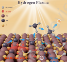
In-Situ and Non-Destructive Hydrogen Plasma Cleaning of Sn from the Protection Layers of Euv Mirrors: The Mechanisms of Surface Interaction.
Abstract
EUV lithography technology, capable of achieving 2 nm nodes, faces challenges of reduced reflectivity caused by Sn deposition on EUV mirrors. RuO2 has demonstrated superior performance as a protective layer for EUV mirrors. This study employs density functional theory (DFT) calculations and plasma cleaning experiments to assess the efficacy of hydrogen plasma in removing Sn contaminants from RuO2 surface. Theoretical results indicate that Sn desorption from RuO2 surface occurs via interactions with hydrogen atoms, transitioning Sn from a metallic state to an H-hybridized molecular state. Experimental findings confirm that RuO2 exhibits lower catalytic activity than Ru, mitigating Sn re-deposition induced by SnHx dissociation. Notably, residual Sn on RuO2 surface forms SnO2 crystals due to ion thermal effects. Complete Sn removal and suppression of re-deposition were achieved using a combination of superficial blowing and enhanced active particle methods. However, compared to Ru, reducing H atoms in RuO2 induces oxygen vacancies, severely degrading its performance. Based on the properties of Ru/RuO2, this study identifies TiO2 as a promising protective layer, exhibiting efficient cleanability (for Sn), resistance to re-deposition, and strong reduction stability, as preliminarily validated by experiments. These findings provide valuable insights into the maintenance of EUV mirrors and the selection of protective coatings.

Wuhan Optics Valley releases new software industry policy, with up to 300 million yuan in support for EDA sector
Wuhan East Lake Hi-Tech Zone issued "Several Measures of East Lake Hi-Tech Zone to Accelerate the Innovation and Development of Software and Information Technology Services Industry" (hereinafter referred to as "Several Measures"), which contains 14 specific measures, including further support for the layout of artificial intelligence and the construction of open source ecology.
The "Several Measures" proposes to build an innovation platform in the field of industrial software. Support key enterprises to take the lead in building technology innovation or industrial ecological service platforms for industrial software (EDA, CAX, etc.) around domestically produced independent control. For platforms with a total investment of more than 100 million yuan, strong industrial driving effects and in line with the national key development strategy, support will be provided according to 50% of the annual construction investment of the platform. The annual support amount for a single platform shall not exceed 100 million yuan, and the cumulative amount shall not exceed 300 million yuan.
The "Several Measures" proposes to build an innovation platform in the field of industrial software. Support key enterprises to take the lead in building technology innovation or industrial ecological service platforms for industrial software (EDA, CAX, etc.) around domestically produced independent control. For platforms with a total investment of more than 100 million yuan, strong industrial driving effects and in line with the national key development strategy, support will be provided according to 50% of the annual construction investment of the platform. The annual support amount for a single platform shall not exceed 100 million yuan, and the cumulative amount shall not exceed 300 million yuan.
Corell received tens of millions of yuan in A+ round financing, focusing on the IGBT/SiC module packaging equipment track
According to Hard Krypton, Corell Technology (hereinafter referred to as "Corell") recently announced that it has completed a tens of millions of yuan A+ round of financing. The investor is Zhejiang Venture Capital, and the funds will be used for product research and development and operating capital replenishment.
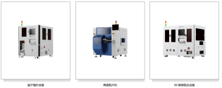
Founded in 2014, Corell provides full-line solutions with medium and high power IGBT/SiC module packaging equipment as its core, including more than ten core products such as high-precision placement machines, fully automatic micron-level pin insertion machines, and SiC flip-chip bonding equipment.
In 2021, Corell developed domestic energy storage-grade and automotive-grade IGBT module packaging equipment, which can package IGBT/SiC chips into modules with specific functions and performance to meet the flexible needs of different customers in different scenarios. The company has a number of core products, among which the TP-3000-HG series high-speed placement machine is based on the high-speed placement of SiC module chips. The overall modular design can achieve a placement accuracy of less than 3 microns and can support 6-inch, 8-inch and 12-inch chip placement.
