这是国际上首次将高温超导技术应用于磁控直拉单晶生长,为高温超导技术产业化做了很多开创性的工作,开辟了超导技术产业化新赛道
Worlds first high temp superconducting magnet heated Cz Si boule for semi wafers
这是国际上首次将高温超导技术应用于磁控直拉单晶生长,为高温超导技术产业化做了很多开创性的工作,开辟了超导技术产业化新赛道
Thabks. The guy @BoraTas replied to him last year saying his claim was about SMEE's backend scanners and that they have had a .75 NA lens for years, and he didn't deny it... he just bragged about how many bookmarks and impressions he got and is promoting his news aggressor website. He got asked again today if he still agreed with his assessment from last year about the SMEE lens and he again dodged the question. I think this guy is knowledgeable but I'm getting ever so slight troll vibes as well.
Who the fuck cares, better for the world to underestimate China until Techinsights actually has a Chinese 2nm GPU in their lab for a teardown. All the China doomers are actually a good thing for China, by feeding the public and the government misinformation. Just look at the amount of shit China has gotten away with due to the whole 'There's no way China can innovate, they are 20 years behind us, this sanctions will finish them for good' attitude that results in piecemeal sanctions that just motivate the chinese semiconductor sector more, rather than an actually massive sanction package early on that could actually hurt China.That guy is a fraud and he isn't hvpc. Me and especially @latenlazy have argued against that guy once. He was insisting that NA in optics was about the mirror size. That is not true and NA is one of the first things optics specialists learn. He kept on doubling down despite people posting resources. Then he broke down and posted a self-aggrandizing Tweet series. He then stalked latenlazy for months.
We believe he is a marketer in an SME company at best. A total fraud at worst. What's certain though, he is no engineer related to lithography and he isn't close to any such person.


Putting the picture of the researcher is unnecessary.New progress in the research and development of 13.5nm extreme ultraviolet lithography light source in China—— Breakthrough in high conversion efficiency
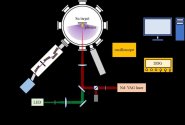
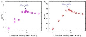
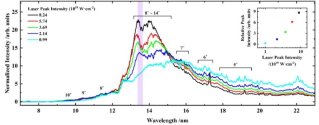
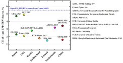
Lin Nan's team from the Shanghai Institute of Optics and Precision Mechanics, Chinese Academy of Sciences, has achieved a 3.42% conversion efficiency of 1 μm solid laser to 13.5 nm extreme ultraviolet light on the laser-driven plasma extreme ultraviolet (LPP-EUV) light source experimental platform they established, and the single pulse energy of 13.5 nm extreme ultraviolet at the main focus exceeded 20 mJ, which is at the international and domestic leading level. The LPP-EUV light source experimental platform established and the research results of the new mechanism of extreme ultraviolet generation by laser plasma carried out with the help of this platform provide technical support for the localization research and development of solid laser-driven LPP-EUV lithography light sources, which is of great significance for China to independently carry out the research and development of EUV lithography and its key devices and technologies.
View attachment 148098View attachment 148100
View attachment 148099
View attachment 148101
View attachment 148103
