Wait, are they saying CXMT is charging more than even Samsungs already overpriced memory chips ?
demand for CXMT and YMTC chips is just so high. more expansion, more LTA with big players like ByteDance and Tencent.

You are using an out of date browser. It may not display this or other websites correctly.
You should upgrade or use an alternative browser.
You should upgrade or use an alternative browser.
Chinese semiconductor thread II
- Thread starter vincent
- Start date
Naura Technology Group empowers Chipsource Microelectronics' front-end coating and developing equipment, promising large-scale production.
The latest financial report shows that Sinyuan Micro achieved operating revenue of 1.948 billion yuan in 2025, a year-on-year increase of 11.11%. In the first quarter of 2026, revenue reached 331 million yuan, a year-on-year increase of 20.08%, with a significant increase in gross profit margin to 46.69%, a year-on-year increase of 12.4 percentage points. New orders also saw substantial growth. Company updates indicate that North China Microelectronics became the controlling shareholder in June 2025.
A research report suggests that the synergistic effect after North China Microelectronics' acquisition is significant. The report points out that North China Microelectronics has comprehensively empowered the company, significantly improving its internal refined management level. Leveraging shareholder resources, the company is focusing on tackling front-end track equipment, accelerating the batch introduction of high-end front-end chemical cleaning equipment to clients, and continuously consolidating its industry position in back-end advanced packaging equipment.
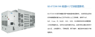
The report believes that the company's strategic positioning in front-end coating and developing core equipment in wafer manufacturing is crucial, as the global market has long been monopolized by overseas companies, with a relatively low domestic production rate. Under the trend of supply chain self-control, domestic wafer fabs are accelerating the introduction of domestically produced equipment. As one of the few domestic manufacturers capable of providing mass-produced front-end coating and developing machines, the company has consistently secured orders from leading wafer foundries since 2025. Multiple equipment models have demonstrated excellent performance in mass production verification, leading to continuously increasing customer recognition.
The research report points out that leveraging the resources of the Naura Technology Group platform, the rapid expansion of downstream demand will drive simultaneous growth in the company's chemical cleaning and bonding equipment. Net profit attributable to the parent company is projected to reach 223 million, 388 million, and 677 million yuan in 2026, 2027, and 2028, respectively. The increased production volume of core equipment, coupled with a shift in gross profit margin, will be key drivers of the company's rapid performance growth.
Feilihua expects its first-half profit to increase by 22%-40%, with its semiconductor quartz materials business benefiting from domestic substitution.
Feilihua released its 2026 semi-annual performance forecast, expecting to achieve a net profit attributable to shareholders of the listed company of RMB 270 million to RMB 310 million in the first half of the year, representing a year-on-year increase of 21.78%-39.82%.
The company stated that the revenue growth mainly benefited from the improved global semiconductor industry and the advancement of the domestic substitution strategy, resulting in steady revenue growth in the semiconductor segment. Meanwhile, in response to the demand for AI computing infrastructure, the company's quartz electronic cloth products continued to advance client-side testing and terminal certification.
As a domestic semiconductor quartz material supplier, Feilihua continues to invest in high-purity quartz products and related materials, and is expected to benefit from the expansion of wafer manufacturing and the trend of localization of the semiconductor industry chain.
Gallium core wafer-level thick-film epitaxial wafers pass device verification, outperforming imported products.
Hangzhou Gallium Core Semiconductor Co., Ltd. has successfully completed a major milestone in semiconductor manufacturing, with its gallium oxide homoepitaxial wafers passing rigorous device verification. In collaboration with Xi'an University of Electronic Science and Technology, the company fabricated terminalless Schottky Barrier Diodes (SBD) using its thick-film epitaxial wafers, which feature a 10 μm epitaxial layer thickness and a carrier concentration of 1×10¹⁶ cm⁻³. The resulting devices demonstrate excellent breakdown voltage and conduction characteristics, with core parameters reaching international advanced levels. This achievement marks a crucial breakthrough for China's large-size gallium oxide materials, moving them from research to reliable device application while currently ensuring a stable stock supply for downstream R&D and mass production.
The performance data reveals that Gallium Core's technology significantly outperforms leading Japanese competitors in key metrics. In terms of voltage handling, the SBD devices exhibit a breakdown voltage range of 1090-1490 V, indicating a low defect density and high reliability suitable for ultra-high voltage applications. Additionally, the specific on-resistance ranges from 2.64.5 mΩ·cm², which is far lower than imported counterparts. This combination allows the devices to achieve an optimal balance between conduction efficiency (low energy loss) and blocking capability, solving a common trade-off in high-performance power semiconductors where improving one parameter often degrades the other.
This breakthrough underscores China's strategic approach to technological self-reliance rather than simply adopting international standards. Gallium Core Semiconductor employs a distinct "Chinese characteristics" path featuring a self-developed casting method that eliminates reliance on expensive iridium crucibles, thereby reducing material costs and enabling independent control over crystal growth thermal fields. By managing the defect density and doping uniformity more flexibly through this proprietary process, the company has achieved precise control over critical parameters such as layer thickness and carrier concentration.
Consequently, the superior performance of these devices validates the reliability of Gallium Core's large-scale thick-film epitaxial processes, effectively ending long-standing dependence on imported high-end gallium oxide materials for domestic use. The company now offers series-based layouts with customizable parameters including epitaxial layer thickness, carrier concentration, and doping type to flexibly meet the diverse requirements of both academic research and industrial mass production, positioning China as a significant player in wide-bandgap semiconductor innovation.
Compound semiconductor equipment manufacturer completes tens of millions of yuan in strategic financing.
Recently, Shanghai Bangxin Semiconductor Technology Co., Ltd. completed a strategic financing round of tens of millions of yuan. The investor in this round was Chuxin Holdings Group. The funds will be mainly used for the iterative research and development and capacity expansion of third-generation semiconductor etching and thin film deposition equipment, and to accelerate the batch introduction of domestic front-end process equipment to customers.
Established in 2020, #Bangxin Semiconductor is a national-level specialized and innovative "little giant" enterprise. Its core focus is on the independent research and development of silicon-based special process equipment and compound semiconductor processing equipment. It has launched a complete range of front-end core equipment, including 6/8/12-inch dielectric etching machines, dry chemical etching equipment, and tungsten thin film deposition equipment. Its products are suitable for third-generation semiconductor wafer manufacturing scenarios such as silicon carbide and gallium nitride, and can meet the mass production process requirements of power devices and radio frequency chips.
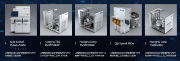
In terms of product commercialization, the company's equipment has passed process verification and achieved mass production in multiple wafer fabs. In 2025, the annual equipment shipment volume will exceed 100 units, and the historical cumulative shipment volume will exceed 200 units. The company has a high domestic market share in the SiC silicon carbide etching equipment sub-segment.
In addition to its headquarters R&D and production base in Lingang, Shanghai, the company is also simultaneously developing the Wuhan Central China Intelligent Manufacturing Base and the Qingdao Industrialization Project. The first phase of the production line of the Qingdao subsidiary has a planned total investment of 200 million yuan, which will further expand the delivery capacity in the northern region and form a supporting synergy with the local integrated circuit industry chain.
Established in 2020, #Bangxin Semiconductor is a national-level specialized and innovative "little giant" enterprise. Its core focus is on the independent research and development of silicon-based special process equipment and compound semiconductor processing equipment. It has launched a complete range of front-end core equipment, including 6/8/12-inch dielectric etching machines, dry chemical etching equipment, and tungsten thin film deposition equipment. Its products are suitable for third-generation semiconductor wafer manufacturing scenarios such as silicon carbide and gallium nitride, and can meet the mass production process requirements of power devices and radio frequency chips.
In terms of product commercialization, the company's equipment has passed process verification and achieved mass production in multiple wafer fabs. In 2025, the annual equipment shipment volume will exceed 100 units, and the historical cumulative shipment volume will exceed 200 units. The company has a high domestic market share in the SiC silicon carbide etching equipment sub-segment.
In addition to its headquarters R&D and production base in Lingang, Shanghai, the company is also simultaneously developing the Wuhan Central China Intelligent Manufacturing Base and the Qingdao Industrialization Project. The first phase of the production line of the Qingdao subsidiary has a planned total investment of 200 million yuan, which will further expand the delivery capacity in the northern region and form a supporting synergy with the local integrated circuit industry chain.
Flow physics and modeling in extreme ultraviolet sources
Abstract
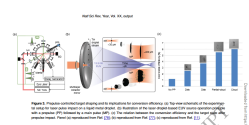
The development of high-power extreme ultraviolet (EUV) light sources based on the laser-produced plasma (LPP) principle is crucial for advanced lithography, enabling the continued scaling of semiconductor devices. However, the underlying processes-involving laser-droplet interaction, plasma evolution, and debris transport-are governed by complex, multiscale, and multiphysics phenomena that pose significant challenges for both simulations and experiments. This review comprehensively surveys recent advances in the flow physics and modeling of LPP-EUV sources, focusing on three key areas: (1) numerical modeling and simulation of laser-tin droplet interaction, including laser absorption, radiation transport, equation of states, etc; (2) progress in understanding droplet dynamics under femtosecond to nanosecond laser pulses; and (3) the flow physics of debris transport and mitigation strategies such as buffer gas jets and magnetic fields. By integrating insights from simulations, experiments, and theoretical analyses, this review aims to bridge the gap between fundamental flow physics and applied EUV source engineering, providing a valuable reference for researchers working toward more efficient and debris-resistant EUV light sources.
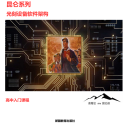
A proposed red book for communist china highschool level in Xinjiang province.
scanner software architecture.
这就是为什么行业内常说:“光刻机不是做出来的,而是算出来的。” 如果没有极为庞
大且精准的数学建模支持,光刻机在开机的一瞬间,高能激光产生的高温就会直接将镜片
光学系统彻底“烤糊变性”,导致成像完全报废。ASML 的强大在于,它不仅有世界上最
顶级的德国蔡司(ZEISS)镜片,更有能够精确预知这块镜片在万分之一秒后会膨胀多少
纳米、并能指挥数万个底层执行器完美将其消减于无形的顶级数学控制软件。硬件给予了
光刻机极限的可能,而极其优秀的数学建模与仿真软件,才真正赋予了光刻机纳米级的灵
魂。
Last edited:
So there is a book called "Lithography Machine Software Architecture" that they tech kids in high school in China? Wow. Most people in school the closer they get in microelectronics is to program a microcontroller for some robot. And in University is a mask aligner or if you are lucky a e-beam machine in a microfabrication lab.
A proposed red book for communist china highschool level in Xinjiang province.
scanner software architecture.
This is why it's often said in the industry: "Lithography machines aren't made, they're calculated." Without extremely large...
With the support of large and precise mathematical modeling, the high temperature generated by the high-energy laser at the moment the lithography machine is turned on directly heats the lens.
The optical system was completely "burnt out," rendering the image unusable. ASML's strength lies in the fact that it not only possesses the world's most advanced technology...
Top-of-the-line German Zeiss lenses can even accurately predict how much the lens will expand in one ten-thousandth of a second.
Nanoscale, and top-tier mathematical control software capable of perfectly reducing tens of thousands of low-level actuators to nothingness. Hardware provides...
The limits of lithography machines are realized, but it is the exceptional mathematical modeling and simulation software that truly endows them with nanometer-scale flexibility.
soul.
View attachment 178794

The link doesn't work
doesnt work? Added a new link above.So there is a book called "Lithography Machine Software Architecture" that they tech kids in high school in China? Wow. Most people in school the closer they get in microelectronics is to program a microcontroller for some robot. And in University is a mask aligner or if you are lucky a e-beam machine in a microfabrication lab.
View attachment 178795View attachment 178796
The link doesn't work
The book is targetting mainly for authur's province, southern Xinjiang. He was named after the kunlun mountain nearby. He figures the west only talk about forced labor and forced concentration camp. He wants shows the development of Xinjiang and his specialty will be added value to to advancement and education of the province.
No, it's not really meant for the rest of China. But feel free if other provinces want to use it.
Nah, micontroller is trivial here. The architecture discussed in book involved maybe hundred of FPGAs controlling thousands of hardwares. PCIe and EtherCat bus..talking about large scale integration needed for euv and duv.
Last edited:
One link is Google drive and another is just regular website. One or both of them should work.