Chinese semiconductor thread II

tokenanalyst

Lieutenant General
Registered Member

Lüliang: Focusing on Promoting the Construction of an Industrial Base Project for Ultra-High Purity Gallium and Downstream Compound Semiconductor Materials​


Lüliang City Mayor Xiong Yizhi unveiled the 2026 government work report, highlighting major advances in industrial development during the 14th Five-Year Plan and setting ambitious goals for 2026 — with a central focus on building a national industrial base for ultra-high purity gallium and downstream compound semiconductor materials.

Key Achievements (14th FYP):​

  • 23 key industrial projects completed across aluminum-magnesium materials, coal chemicals, carbon-based materials, and equipment manufacturing.​
  • 50 major projects signed, including the ultra-high purity gallium and compound semiconductor materials initiative.​
  • Lüliang leads Shanxi Province in revenue from specialized industrial towns and industrial output.​
  • Hydrogen economy breakthrough:
    • 6,000 hydrogen-powered commercial vehicles/year production line.​
    • 14 operational hydrogen refueling stations.​
    • 135,000 tons/year hydrogen production capacity.​
    • Selected as a national fuel cell vehicle demonstration city cluster — the only one in Shanxi.​
  • Strengthened R&D partnerships with top institutions (Huairou Lab, CAS Shanxi Coal Chemistry Institute).​
  • Pilot carbon-based materials base under construction; helium resource lab operational — supporting national strategic projects.​

2026 Priorities:​

  • Dual-track processing strategy: Advance both metallurgical and non-metallurgical industries.​
  • Expand high-purity alumina chain: Ensure full capacity of Tianshuo (200K tons) and Yijiang projects; launch Phase II of Chalco’s 50K-ton alloy and Wenzhuo’s 1.2M auto parts projects.​
  • Core Focus: Accelerate construction of the ultra-high purity gallium and downstream compound semiconductor materials industrial base, with strong support for alumina enterprises to extract and refine all recoverable gallium — positioning Lüliang as a national hub for critical semiconductor raw materials.​
Please, Log in or Register to view URLs content!
 

tokenanalyst

Lieutenant General
Registered Member

The main structure of the Silan Microelectronics headquarters R&D testing and production base project has been completed.​


Recently, the Silan Microelectronics headquarters R&D, testing and production base project was successfully capped in Binjiang District, Hangzhou, marking another important milestone in the company's development. The capping ceremony was held on January 28. Huang Lizhen, Senior Vice President of Silan Microelectronics and Chief Project Commander, Lin Kaitong, Project Manager, and representatives from the general contractor, supervision, design and other participating units attended the ceremony to witness the project's phased achievements.

It is reported that Silan Microelectronics has been continuously increasing its production capacity and R&D investment in recent years, and has established multiple manufacturing bases in Hangzhou, Chengdu, Xiamen and other places, forming a complete industrial chain layout covering chip design, manufacturing, packaging and testing. The Silan Microelectronics headquarters R&D testing and production base is an important strategic project implemented by the company to adapt to business development needs, strengthen its independent design and manufacturing capabilities, and improve its complete industrial chain layout. The project has a total construction area of approximately 96,000 square meters and, upon completion, will become the company's high-end chip R&D testing and verification center, focusing on supporting the development of next-generation power semiconductors, sensors, and high-end analog integrated circuits.

In the future, this base will work in synergy with Silan Microelectronics' manufacturing bases in Hangzhou, Chengdu, Xiamen and other places to further shorten the product cycle from R&D to market and continuously enhance the company's ability to provide efficient, reliable and highly competitive products and services to global customers.

Please, Log in or Register to view URLs content!
 

tphuang

General
Staff member
Super Moderator
VIP Professional
Registered Member

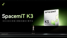
Details on the SpacemiT K3 that just came out.

Support all HF format except for FP4 & FP6 for 30 to 80B param models! 60 TOPS - fully supports 30B-A3B model like Qwen ones. CPU core 2.4GHz, similar to ARM A76 in compute, supports 256bit vector AI core fully support RVA23 & RVV1024 + FP8 inference.

This is a pretty high performing AI focused SoC. 8 AI cores + 8 CPU cores. all using RISC-V
 

tokenanalyst

Lieutenant General
Registered Member

Advanced Spacetime Technology (AST) releases the K3 chip, which leverages the RISC-V architecture to enable new intelligent computing scenarios.​


Advanced Spacetime Technology (AST) has officially launched the K3 chip, the world’s first mass-produced RISC-V CPU compliant with the new RVA23 specification, marking a major milestone in open-architecture computing. Developed over 1,200 days, the K3 represents a quantum leap in performance, AI capability, and ecosystem maturity for RISC-V.​
  • Unprecedented AI Performance: First RISC-V chip to natively support FP8 precision AI inference, delivering 60 TOPS of AI compute.​
  • High-Performance CPU: 8 high-efficiency X100 cores at up to 2.4GHz — single-core performance rivals ARM Cortex-A76.​
  • Breakthrough Parallelism: World’s first 1024-bit wide parallel computing unit on a RISC-V chip.​
  • Chip-Level Virtualization: First RISC-V product with full hardware virtualization support.​
  • Large Model Local Inference: Capable of running 30–80B parameter LLMs locally, with 15 tokens/sec output for 30B models and <1s first-token latency.​
  • Memory & Bandwidth: Supports up to 32GB LPDDR5 memory.​
1769782551139.png

Scenario-Optimized Design:​

  • Robotics: Integrated real-time subsystem with 2 RISC-V RT cores, 3MB cache, and 10 CAN-FD interfaces.​
  • AI & Edge Computing: Full compatibility with Hugging Face models (except FP4/FP6), including Qwen and DeepSeek.​
  • Desktop-Class Responsiveness: Runs Ubuntu, Open Kylin, and open-source HarmonyOS; boots OS and opens browser at speeds comparable to mainstream x86/ARM desktops.​

Full-Stack Ecosystem:​

AST has built a complete RISC-V stack:​
  • Hardware: PICO-ITX SBC, COM260 robot core board, array servers, and open reference designs.​
  • Software: Optimized Linux (Bianbu), compiler toolchains, AI frameworks, and SDKs.​
  • Accessibility: Lowers entry barriers for developers with comprehensive documentation and reference platforms.​

The prior-generation K1 chip shipped 150,000 units by end-2025, establishing AST as a leader in high-performance RISC-V. K3 begins shipping in April 2026, with full technical specs and dev tools released progressively via AST’s website. CEO Chen Zhijian emphasized AST’s unwavering commitment to RISC-V as the foundation for the next-generation open computing ecosystem. “Only by building a full-stack system can we truly empower commercial users and accelerate innovation,” he said With K3’s launch, AST is poised to dramatically expand RISC-V’s footprint in smart terminals, robotics, edge AI, and autonomous systems, challenging traditional architectures and accelerating the global adoption of open-source silicon.​

Please, Log in or Register to view URLs content!
 

tokenanalyst

Lieutenant General
Registered Member

Harbin Founded Suzhou Extreme Ultraviolet Semiconductor Co., Ltd is making progress on Commercial EUV Light Sources.​


Suzhou Extreme Ultraviolet Semiconductor Co., Ltd. has successfully developed a 120W extreme ultraviolet (EUV) light source prototype — a critical breakthrough in China’s quest to overcome the long-standing technological bottleneck in EUV lithography equipment. As EUV lithography is essential for manufacturing advanced chips, global supply restrictions have made domestic EUV light source development a national strategic priority. Founded in 2022, the company, led by plasma expert Professor Zhang Xingqiang, has achieved key milestones including successful discharge tests and filed core patents for innovations like the “dual vacuum light source design” and “capillary discharge plasma-coupled structure,” which enhance output power and purity while reducing operational complexity.

With a 120W output meeting baseline EUV lithography requirements, the company aims to supply domestic chipmakers like SMIC and Shanghai Microelectronics, offering solutions 15–30% cheaper than global leaders ASML and Nikon, while maintaining strong margins. Targeting commercialization by 2026 and mass production by 2030, Suzhou EUV is now seeking financing to refine its prototype and accelerate industrialization. The breakthrough represents not just a technological leap but a pivotal step toward China’s semiconductor self-reliance, with plans to list on the STAR Market. This achievement signals major progress in decoupling China’s chip industry from foreign dependencies.

1769784796403.png
 

jli88

Junior Member
Registered Member
Please, Log in or Register to view URLs content!

Some highlights:

  1. YMTC- Construction on the Wuhan Plant 3, which began in September of last year, was initially expected to begin full-scale production next year. However, local officials predict that YMTC will adjust its schedule and begin mass production in the second half of this year.
  2. YMTC's market share, based on NAND shipments, reached 10% for the first time ever in the first quarter of last year, and rose 4 percentage points year-on-year to 13% in the third quarter.

@tokenanalyst Is this the YMTC fab with rumored 100% domestic equipment?
 
Top