Chinese semiconductor thread II

justinlee

Just Hatched
Registered Member
yes, SSC800 is KRF if you do a search. This is what hvpc said a while back.

At this point, I don't think you need to do a bid for SSA800. You either buy it or you don't.

The key here is that it's considered to be matured and reliable enough that it's going through bids. But IIRC, KRF scanners are around $10m so this is more expensive than imported ones. That tells me they have yet to scale up production. Either that or imports got a lot more expensive.

Please, Log in or Register to view URLs content!
Data from MIIT:
KrF Litho: Wavelength=193mm, Resolution≤65nm, overlay≤8nm

and ASML websites:
TWINSCAN XT:1460K:
Wavelength=193mm, Resolution≤65nm, similar spec, and ask for €12m ~ ¥100m

I think it's fair enough after tax :D
 

justinlee

Just Hatched
Registered Member
If those are the numbers MIIT provided then it’s not KrF.
Sry my mistake. I accidentally copy paste ArF litho spec on MIIT website.

ERRATA
具体来看,氟化氪光刻机晶圆直径为300mm(12英寸);照明波长为248mm;分辨率≤110nm;套刻≤25nm

TWINSCAN XT:1460K:
similar spec, and ask for €12m ~ ¥100mIMG_3946.jpeg
 
Last edited:

PopularScience

Senior Member
Registered Member
Sry my mistake. I accidentally copy paste ArF litho spec on MIIT website.

ERRATA
具体来看,氟化氪光刻机晶圆直径为300mm(12英寸);照明波长为248mm;分辨率≤110nm;套刻≤25nm

TWINSCAN XT:1460K:
similar spec, and ask for €12m ~ ¥100mView attachment 166887
notice the overlay accuracy improved to <= 15nm

95b1bf003af33a87975c6400805c10385343b57b.jpg
 

tokenanalyst

Lieutenant General
Registered Member

Dongfang Jingyuan's competitive advantage in the new generation HV-SEM output electron beam quantity detection continues to be strengthened.​


Recently, the first unit of SEPA®-h755, a new generation of high-energy electron beam measurement equipment (HV-SEM) independently developed by Orient Crystal Source, was successfully delivered to a leading domestic customer. The HV-SEM is Orient Crystal Source's fourth electron beam metrology testing device, following EBI, CD-SEM, and DR-SEM, marking the company's comprehensive layout in the four core areas of front-end electron beam metrology equipment. The successful delivery of the new generation HV-SEM not only further consolidates the company's leading advantage in this domestic market but also demonstrates its core technological strength in electron beam metrology testing for advanced processes.
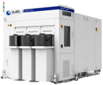
1766757722147.png

The core of high-energy electron beam (HEEB) equipment lies in its use of high-energy electron beams for scanning imaging. The landing energy of these electron beams typically reaches 30 keV or higher, far exceeding the conventional level of 5 keV or lower for other electron beam quantity detection equipment. This ultra-high landing energy endows the equipment with the ability to "see through" deep within the wafer for imaging. However, this requires overcoming a series of technical challenges, including high-voltage systems, high-energy electron beam deflection and precise control, multi-detector synchronous imaging, high-speed and high-precision motion control platforms, special scene calibration techniques, standard sample preparation, and the development of novel software algorithms. Leveraging its profound technical expertise in the electron beam field, the R&D team at Orient Crystal Source overcame these difficulties, successfully launching this new equipment and achieving rapid technological iteration and upgrades.

Looking back at the R&D process, Dongfang Jingyuan officially launched the HV-SEM R&D project in early 2024. That year, the team overcame the challenges of 30keV landing energy electron beam imaging technology, completed the overall application process setup and core algorithm development, and validated it in a real-world wafer fab scenario. In April 2025, the team successfully achieved 45keV high-energy electron beam imaging, with core indicators reaching the standards of leading international products. In December 2025, the equipment completed application demo testing in high-end process technologies such as 3D-NAND, DRAM, and advanced logic, fully demonstrating its measurement capabilities for 3D structures in advanced processes.

HV-SEM has unique application value and can play a key role in advanced processes and specialty technologies:

1. SEM Overlay Measurement:
High-energy electron beams have a certain material penetration depth. Combined with a BSE (backscattered electron) detector, they can capture micron-level depth signals of the sample, achieving "see-through" imaging. By combining this with sample surface information acquired by an SE (secondary electron) detector, positional difference analysis of the structure in the two images can be performed, accurately completing SEM overlay (alignment or overlay precision) measurements. Actual measurement data shows that the SEpA®-h755 can clearly display the first three metal layers within a 1μm field of view on the Metal HMET layer.
1766757744740.png

2. High Aspect Ratio (HAR) Structure Measurement: For structures with an aspect ratio greater than 10:1, such as deep holes and deep trenches, a high-energy electron beam can be incident on the bottom of the structure and feed back an effective signal to the detector, thereby achieving imaging and measurement. Currently, the equipment has completed high aspect ratio measurement verification for two-dimensional structures with a ratio of 30:1 and one-dimensional structures with a ratio of 80:1.

3. Expanding Defect Detection Applications: Leveraging the advantages of high-energy electron beam technology, it is possible to achieve expanded detection applications such as special types of defects.

4. Big Data Visualization and Analysis: Equipped with big data visualization software independently developed by Oriental Crystal Source, it can conduct overall trend analysis of CDU and OVL, providing data support for process optimization.
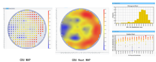

1766757765866.png

Please, Log in or Register to view URLs content!
 

tokenanalyst

Lieutenant General
Registered Member

With a total investment of approximately 5 billion yuan, Xinmei Materials' Hefei project will begin mass production next year after equipment is moved in.​


December 25th, the equipment move-in ceremony for the Xinmei Materials· Xin Station Optical Functional Film Project was held in Hefei New Station High-tech Zone. The move of this core equipment marks a significant milestone in the project's construction, effectively guaranteeing Xinmei Materials' increased production capacity and market supply, accumulating experience for subsequent intelligent upgrades of the production line, and further accelerating the localization process of high-end optical functional films in my country. Once fully operational, the project will significantly enhance the domestic self-sufficiency in key materials for the optoelectronic display industry chain.

The Xinmei Materials Xinzhan Optical Functional Film Project has a total investment of approximately 5 billion yuan and plans to build five internationally leading intelligent display material production lines, including two precision protective film production lines, two surface coating production lines, and one P0 production line, covering key raw materials for LCD/OLED polarizers and OLED supports. Construction of the project commenced in March of this year, and the main structure of the factory was completed in November of the same year. With the first batch of core equipment officially moved in, it is expected to enter the trial production stage in April 2026 and achieve mass production in the third quarter of 2026.

Please, Log in or Register to view URLs content!
 

tokenanalyst

Lieutenant General
Registered Member

ESW Computing and Canonical sign a licensing agreement to promote the integration of open-source software and hardware ecosystems.​


ESW Computing has entered a strategic licensing agreement with Canonical, the company behind Ubuntu, enabling its EBC77 series hardware comprising the SBC single-board computer and Mini-DTX motherboard to officially support and ship with the Ubuntu operating system. This collaboration strengthens the integration of open-source software and hardware ecosystems, offering developers a seamless, out-of-the-box experience and boosting development efficiency.

Products covered:​
  • EBC77 SBC Single-Board Computer:
    Compact (85mm×56mm), powered by ESWITCH’s self-developed RISC-V SoC EIC7700X (quad-core RISC-V CPU + 20TOPS NPU), 16GB LPDDR5 memory, and capable of running large language models like Qwen and DeepSeek locally. Fully compatible with Ubuntu (available on GitHub), it supports plug-and-play deployment in smart education, edge computing, and embedded AI applications.​
  • Mini-DTX Motherboard:
    High-performance platform (203mm×170mm) featuring the industry’s first die-to-die interconnect RISC-V chip EIC7702X (8-core 64-bit CPU + 40TOPS NPU), 32/64GB LPDDR5 memory, and rich I/O for industrial sensors and HD cameras. Ships pre-installed with Ubuntu, ideal for AI PCs, machine vision, and intelligent video analytics.​
  • HiFive Premier P550 Development Board:
    A flagship RISC-V platform co-launched by SiFive and ESW Computing, featuring a quad-core SiFive P550 CPU (up to 1.8GHz), 20TOPS NPU, 32GB LPDDR5 memory, 128GB eMMC storage, and PCIe/SATA interfaces. Comes with Ubuntu, GCC/LLVM toolchain, and open-source SDK—perfect for IoT, robotics, and AI edge computing projects.​

1766758611063.png

Please, Log in or Register to view URLs content!
 

tokenanalyst

Lieutenant General
Registered Member

AMEC's innovative achievements have won two major awards: the Jiangxi Provincial Patent Award and the Gold Award at the Height Increase Competition.​


Advanced Micro-Fabrication Equipment Inc. (AMEC) has been honored with two major national awards for its groundbreaking innovations in semiconductor equipment. The company received the Jiangxi Provincial Patent Award for its invention patent, “Chemical Vapor Deposition Reactor or Epitaxial Layer Growth Reactor and its Support Device” (inventors: Yin Zhiyao and Jiang Yong). This patented technology solves long-standing challenges in Metal-Organic Chemical Vapor Deposition (MOCVD) systems such as substrate slippage and thermal deformation by introducing a novel dual-structure design that uses pushing-force transmission and a large-area support surface. These advancements ensure precise, stable, and reliable performance under high-temperature conditions, significantly enhancing process accuracy and production efficiency.

In addition to this recognition, AMEC clinched the Gold Medal and top ranking in the 2nd “Changgao Competition,” a prestigious national contest organized by the State Intellectual Property Office and provincial authorities along the Yangtze River Economic Belt. The win was based on another core patent: “Gas Spray Head, Its Manufacturing Method and Thin Film Growth Reactor.” Out of 1,410 projects from 11 provinces, AMEC stood out through exceptional technical depth and strategic application, highlighting its leadership in high-value patent commercialization and industrial transformation.

The impact of these innovations is evident in AMEC’s advanced product lineup, including PRISMO D-BLUE®, HiT3®, PD5®, and the latest-generation PRISMO UniMax® systems. These MOCVD platforms are now market leaders—especially PRISMO UniMax®, which commands over 90% share in Mini LED backlight and direct-view epitaxial wafer production. Backed by a fully integrated R&D and manufacturing base in Nanchang (completed in July 2023), AMEC has established itself as a key player in China’s semiconductor equipment ecosystem, earning accolades such as National High-tech Enterprise and Jiangxi Provincial Manufacturing Single Champion status.

Beyond technological excellence, AMEC is driving sustainable development its equipment enables LED products that consume over 70% less energy than traditional lighting, supporting global green initiatives. Guided by its “Five Tens” corporate culture and a clear vision to become a world-class equipment enterprise, AMEC continues to invest heavily in R&D and innovation. With a balanced strategy of organic growth and external expansion, the company is accelerating toward becoming a globally competitive leader in high-end micro-fabrication equipment.
Please, Log in or Register to view URLs content!
 
Top