You are using an out of date browser. It may not display this or other websites correctly.
You should upgrade or use an alternative browser.
You should upgrade or use an alternative browser.
Chinese semiconductor thread II
- Thread starter vincent
- Start date
what is CETC working on in it's labs?
This is like the forefront of research. GaN-on-Diamond & carbon nanotube electronics seem especially interesting to me
so new integrated chips (sounds like advanced packaging to me), new GaN module & IC, GaN-on-Diamond, microwave photon and Carbon based electronics.发展新质生产力,根本上取决于科技创新能力,特别是关键核心技术的创新突破能力。”着力攻关异质集成技术,团队首次提出并实现基于异质集成架构的大功率芯片,突破小体积、高功率、低损耗瓶颈。目前,正聚焦芯片级异质集成、新型GaN器件及电路、金刚石基GaN、微波光子、碳基电子等领域,推进关键核心技术攻关和应用技术创新。
This is like the forefront of research. GaN-on-Diamond & carbon nanotube electronics seem especially interesting to me
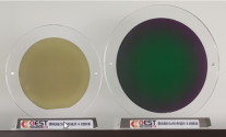
Baishi Electronics completed the A+ round of financing to accelerate the layout of high-voltage, large-size third-generation semiconductor epitaxy
Recently, Nanjing Baishi Electronic Technology Co., Ltd. completed the A+ round of financing. Many well-known institutions participated in the investment, and China Venture Capital served as financial advisor.
Baishi Electronics was founded in 2019 by a number of senior experts with decades of experience in third-generation semiconductor epitaxy. The core team has full-stack capabilities such as epitaxial process development, yield assurance, and equipment improvement. The company's first production line is located in Pukou District, Nanjing City. It will be put into production in 2021. The current annual production capacity reaches 50,000 pieces, and its customers are mostly global giants and domestic leaders. The company plans to build a second-phase production line in the Yangtze River Delta in the near future, with a planned production capacity of 280,000 wafers per year, to build the country's leading automotive-grade third-generation semi-epitaxial wafer manufacturing plant.

Baishi Electronics relies on its team's strong mass production experience and high-quality manufacturing capabilities to provide six-inch and eight-inch epitaxial wafers to meet the market demand for power devices in the new era. In addition to standard specification epitaxial wafers, Baishi Electronics can provide customized specification epitaxy services and key processes required for device development based on special application market needs.
The thickness, concentration and number of surface defects of the silicon carbide epitaxial layer will affect the electrical characteristics of the device, resulting in a loss of silicon carbide device yield. At present, general epitaxy technology can only control killer defects with large surface sizes (such as triangular defects, carrot defects, linear defects, comet defects, etc.), with a density of about 1/cm2, and the number of micro-pits on the surface. Up to more than 5,000 pieces per piece. Baishi's unique epitaxial technology can effectively control the number of surface defects to a density of less than 0.4/cm2, and surface micro-pits (micro-pits) < 1,000/wafer. It also has low fatal defects and surface micro-pits. hole advantage. In 2023, Baishi epitaxial processes and technical levels will continue to improve. 3,300V silicon carbide epitaxial wafers will achieve high-yield and high-quality production, with product thickness uniformity of 1.18% and concentration uniformity of 1.32%, and will be stably shipped to global rail transit customers. Ultra-high voltage (6,500V and above) epitaxial technology continues to make breakthroughs, and defect control has reached the internationally advanced level.
Huazhuo Jingke applied for patents for motion platforms and semiconductor manufacturing equipment to improve semiconductor processing accuracy and processing efficiency.
According to news from the financial industry on March 8, 2024, according to the announcement of the State Intellectual Property Office, Beijing Huazhuo Jingke Technology Co., Ltd. applied for a project called "Motion Platform and Semiconductor Manufacturing Equipment", with the public number CN117672950A, and the application date is August 2022. moon.
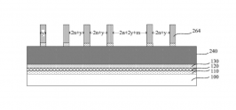
The patent abstract shows that the present invention provides a motion platform and semiconductor manufacturing equipment, and relates to the field of semiconductor technology. The motion platform includes a base and a cover located on the base. A rotating drive component is installed on the top support surface of the base. The rotating drive end of the rotating drive component is connected to a lifting mechanism. The rotating drive component is located in the cover. The top plate of the cover An opening is provided for the lifting drive end of the lifting mechanism to extend. The semiconductor manufacturing equipment includes a substrate and the above-mentioned motion platform, and the substrate is installed on the lifting drive end of the lifting mechanism of the motion platform. The lifting drive end of the lifting mechanism in this motion platform directly carries the workpiece to be processed through the base plate, without bearing the weight of the rotating mechanism, thereby effectively reducing the driving load of the lifting drive component, correspondingly improving its start-stop response speed and accuracy, thereby improving the motion platform The response speed and position drive accuracy, as well as the processing accuracy and processing efficiency of semiconductor manufacturing equipment.
outdated information ..China still using alot of US bridge switch for its aircond. self suffiency drive should include this type. This is old stuff.
Chinese military hardwares probably use US bridge switch too.
we have confirmation from AVIC itself, back in 2021. Zhuhai air show. Chinese military industrial complex have replaced all foreign parts in semiconductor supply chain include all software too. its now 100 percent domestic.
AccoPower, which likely has contract with GAC Aion, BAIC and Geely started production at it 7.5B RMB plant in Guangdong. Already has 10k wpm of production capacity. Delivered tape outs to 40+ customers
Goal is to achieve 240k wpm 6-inch production by this year and convert that to 8-inch eventually
Goal is to achieve 240k wpm 6-inch production by this year and convert that to 8-inch eventually


