Chinese semiconductor thread II

henrik

Senior Member
Registered Member
CXMT has launched the latest DDR5 product line: maximum speed of 8000Mbps and maximum chip capacity of 24Gb.
with 7 new modules and products, including UDIMM, SODIMM, CUDIMM, CSODIMM, RDIMM, MRDIMM and TFF MRDIMM, meet all application needs such as servers, workstations and personal computers.


View attachment 165165

When will we see ddr5 ram prices going down worldwide?
 

tphuang

General
Staff member
Super Moderator
VIP Professional
Registered Member
When will we see ddr5 ram prices going down worldwide?
not for a while


Please, Log in or Register to view URLs content!

Wuhan is becoming China's 5th semiconductor city after Beijing, Shanghai, Shenzhen and Wuxi. During the 15th FYP, it plans to become major storage capital and has JFS lab as a major research facility. Plans to build 10 new fabs with total production of 500k wpm overall.

Wuhan optical valley is a major center of optical chips production. A major local champion is 长飞光纤/Yangtze optical fiber and cable.
 

tokenanalyst

Lieutenant General
Registered Member

Yanwei Semiconductor completes hundreds of millions of yuan in Series A financing to accelerate the domestic substitution of high-end thin film deposition equipment.​


Yanwei (Jiangsu) Semiconductor Technology Co., Ltd. has successfully closed a Series A financing round of several hundred million yuan, with investors including Yongxin Ark, Jinyuan Capital, and Hefei Industrial Investment. Founded in 2022 in Wuxi, the company specializes in high-end semiconductor equipment development focusing on atomic layer deposition (ALD), Si epitaxy (SI EPI), PECVD, SiC epitaxy (SiC EPI), and atomic layer etching (ALE with a strong emphasis on independent IP and international competitiveness.

As logic and 3D memory chip processes advance, ALD technology is critical for high-precision, uniform thin film deposition in sub-45nm nodes and advanced packaging. Facing reliance on foreign equipment due to geopolitical restrictions, Yanwei has achieved breakthroughs in niche areas like tALD, PEALD, and low-voltage EPI, enabling domestic substitution and establishing a competitive edge.

The company’s core team brings rare global expertise across NAND, DRAM, and logic equipment development, allowing it to go from inception to full fab validation in just three years a feat recognized as highly efficient within the industry. The raised funds will support further R&D and team expansion, advancing China’s self-reliance in critical semiconductor manufacturing technologies.

Please, Log in or Register to view URLs content!
 

tokenanalyst

Lieutenant General
Registered Member

Yifeng Smart Chip's advanced packaging project lands in Luohu, Shenzhen.​

Luohu ushered in an important milestone in the development of its semiconductor industry—the signing ceremony for the Yifeng Smart Chip Advanced Packaging Project, jointly initiated by Luohu Investment Holdings, Yidao Information, and Huafeng Technology, was held.

The Yifeng Smart Chip project, which has been launched this time, will focus on cutting-edge technologies such as 2.5D and 3D packaging and fully environmentally friendly processes. It will focus on AI hardware and smart wearable devices such as robots (embodied intelligence), AR/VR products, AI glasses, and smartwatches, and accurately solve the core needs of AI terminals for "miniaturization, low power consumption, and long battery life".

According to reports, E-Feng Smart Chip's advanced packaging production line will adopt cutting-edge technologies such as glass substrates, 2.5D and 3D packaging, and fully environmentally friendly processes. It is committed to meeting the advanced packaging needs of domestic chip manufacturers, PCB manufacturers, and end customers, promoting innovation in AI hardware and smart wearable devices such as robots (embodied intelligence), AR/VR products, AI glasses, smartwatches, portable laptops, and headphones, and solving the core needs of AI+ terminals and AI+ applications in terms of miniaturization, low power consumption, and long battery life.

At the ceremony, representatives from the Luohu District Government, Yidao Information, and Huafeng Technology jointly signed an agreement, marking the official launch of the tripartite cooperation. As one of the project partners, Luohu will fully leverage its guiding role, integrate local industrial resources, and provide comprehensive service guarantees for the project, helping enterprises quickly achieve production capacity implementation and technology transfer.

Please, Log in or Register to view URLs content!
 

tokenanalyst

Lieutenant General
Registered Member

Three chip-related funds have been officially approved.​

16 public funds focusing on hard technology were approved, including three products from E Fund Management: E Fund CSI Science and Technology Innovation Board Artificial Intelligence ETF, E Fund SSE Science and Technology Innovation Board Chip ETF, and E Fund SSE Science and Technology Innovation Board Chip Design Theme ETF.

Specifically, products such as the E Fund CSI Science and Technology Innovation and Entrepreneurship Artificial Intelligence ETF track the CSI Science and Technology Innovation and Entrepreneurship Artificial Intelligence Index, focusing on core links of the AI industry chain, including basic resource fields such as optical communication and domestic AI chips, as well as AI technology and application links, and packaging core listed companies in the innovation and entrepreneurship sector in one go.

The other two funds both focus on the chip industry. The E Fund SSE STAR Market Chip ETF tracks the SSE STAR Market Chip Index, covering all aspects of the chip industry chain, including chip design, manufacturing, packaging and testing, and equipment, reflecting the overall development trend of the semiconductor industry. The E Fund SSE STAR Market Chip Design Theme ETF tracks the SSE STAR Market Chip Design Theme Index, which selects companies engaged in chip design on the STAR Market, targeting high-value-added segments of the industry chain. For investors interested in the chip industry, these two ETFs offer differentiated investment options.

In recent years, E Fund Management has continued to increase its investment in "hard technology" ETF products, and has launched products such as the STAR Market 50 ETF, Artificial Intelligence ETF, STAR Market Growth 50 ETF, and E Fund SSE STAR Market Chip Index Fund, covering different types such as broad-based, industry-themed, and style factor, providing diversified investment options for investors both on and off the exchange.

Please, Log in or Register to view URLs content!
 

tokenanalyst

Lieutenant General
Registered Member

Apex: Empowering the Upgrading of the Wet Electronic Chemicals Industry with High-Purity Process Equipment Innovation​


Apex Technology, a Shanghai-based innovator in high-purity process equipment for wet electronic chemicals, has been nominated for the prestigious IC Power List Annual Most Promising Growth Award at the 2026 IC Awards recognizing its rapid rise and technological breakthroughs in semiconductor and new energy materials. The awards, expanded this year to include 73 categories across nine sectors, are judged by over 100 semiconductor industry leaders and 500 CEOs.

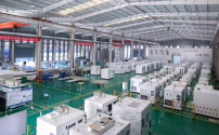
Apex specializes in designing and manufacturing core system equipment for the production of ultra-pure chemicals essential in chip fabrication and battery manufacturing. Its comprehensive solutions span compounding, purification, synthesis, and supporting auxiliary systems—delivering end-to-end, contamination-free processes from raw materials to final packaging. Key capabilities include producing G4/G5 grade acids (e.g., hydrofluoric, sulfuric, nitric acid) and synthesizing critical reagents like photoresists and etching solutions.

High-Purity Purification Process System

At the heart of semiconductor-grade chemical production lies purity—critical for preventing defects in nanoscale chip manufacturing. Apex’s advanced purification systems are designed to deliver ultra-high-purity reagents at G4 and G5 levels (the highest tiers in industry standards), directly addressing the growing needs of 3nm and below process nodes.

The system specializes in purifying critical raw materials including:​
  • Hydrofluoric acid (HF): Achieving G4/G5 purity for etching applications.​
  • Hydrogen peroxide (H₂O₂): Produced at G3/G5 levels for safe, effective cleaning and oxidation processes.​
  • Sulfuric acid (H₂SO₄): Purified to G4/G5 grades with stringent metal ion control (<10 ppb).​
  • Nitric acid (HNO₃): Electronic-grade nitric acid meeting ultra-low particulate and metallic impurity specifications.​
  • Hydrochloric acid (HCl) & other halogens: Processed through multi-stage filtration, distillation, and deionization to ensure reliability across sensitive applications.​
These systems employ closed-loop design principles, advanced membrane filtration, ion exchange resins, and real-time monitoring of particle counts (<0.1μm), enabling consistent output quality essential for high-volume production environments.​

High-Purity Mixing Process System

Precise formulation is vital to the performance of wet chemicals used in photolithography, cleaning, etching, and polishing processes. Apex’s mixing systems are engineered for extreme accuracy, reproducibility, and contamination control—ensuring stable batch-to-batch consistency.​
  • Multi-component dosing technology with micron-level precision.​
  • Integration of real-time particle monitoring, online pH/temperature sensors, and automatic calibration mechanisms.​
  • Compatibility with a wide range of critical reagents such as:
    • Photoresists and diluents​
    • Developers and stripping solutions (for post-exposure development)​
    • Etching solutions (e.g., HF/HNO₃ mixtures for silicon etch)​
    • Cleaning agents (SC1/SC2, RCA clean formulations)​
    • CMP slurry preparation systems​
    • Electroplating baths (Cu, Ni, Co) for advanced interconnects​
The system also incorporates dedicated canning stations with nitrogen purging and sealed transfer paths, along with ultra-fine filtration modules (0.1μm/0.05μm)to prevent particle contamination during dispensing—ensuring zero secondary pollution even in the final packaging stage.
1763997156496.png

High-Purity Synthesis Process System

For complex chemical synthesis required in semiconductor materials like photoresists, polymers, and functional additives, Apex delivers fully integrated, modular synthesis platforms capable of executing sensitive reactions under controlled conditions.

This system supports:​
  • Polymerization (e.g., for resist resins)​
  • Esterification & Transesterification (to tailor molecular weight and solubility profiles)​
  • Acid-base neutralizations, condensation, and catalytic reactions
Applications include the production of:​
  • Positive and negative photoresist formulations​
  • Stripping agents for advanced patterning layers​
  • Cleaning solutions with tailored surface tension properties​
  • The system is designed as a fully automated, end-to-end solution—from raw material feeding and controlled reaction (with temperature/pressure regulation) to final concentration via vacuum distillation, multi-stage filtration, degassing, and sterile packaging. This seamless integration reduces human intervention, minimizes batch variability, and enhances traceability.​
1763997194574.png

Supporting Auxiliary Systems

To ensure continuous, stable operation across long production runs, Apex provides critical auxiliary systems:
  • Solid-Liquid Separation Units: High-efficiency centrifuges and membrane filters for removing residual solids without introducing contamination.​
  • High-Purity Powder Drying Systems: Used in the processing of dry chemical intermediates, featuring inert gas (N₂) flushing to prevent oxidation or moisture absorption.​
  • Degassing Towers: Equipped with vacuum-assisted systems that eliminate dissolved gases (e.g., O₂, N₂) from liquids—vital for preventing bubble formation during etching and deposition.​
These components are designed to operate in ultra-clean environments and seamlessly integrate into the main process flow, improving overall system uptime and product yield.​

Core Equipment & Customized Cabinets

Apex manufactures specialized high-performance equipment built with materials resistant to aggressive chemicals:
  • Corrosion-resistant reactors made from PTFE-lined stainless steel or specialty alloys (e.g., Hastelloy C276).​
  • High-efficiency heat exchangers for precise temperature control during reactions.​
  • Filter tanks and precision valves designed for long-term durability under high-purity conditions.​
The company also develops customized cabinets tailored to specific workflow needs, including:
  • Liquid feeders with zero-leak seals​
  • Particle removal filtration process cabins (classified as Class 100 cleanroom-compatible)​
  • Automated filling stations supporting diverse container sizes—from small 4L/20L drums to large 200L and 1,000L tank trucks​
These cabinets are engineered with sealed transfer pathways, inert gas purging, and real-time monitoring, ensuring that chemical integrity is maintained throughout transport and delivery critical for preventing post-processing contamination.​

Closed-Loop Solutions & End-to-End Service Ecosystem

Beyond hardware, Apex delivers a comprehensive service model rooted in collaboration and lifecycle support:
  • Strategic partnerships with global industry leaders such as DuPont, Daikin, ALMATEC, Milton Roy, and Entegris, enabling seamless integration of best-in-class components.​
  • A full-service approach: from initial needs assessment and customized engineering design to installation, commissioning, training, and long-term after-sales maintenance & technical support.​
All systems comply with international standards:
  • ISO 9001 (Quality Management)
  • ISO 14001 (Environmental Management)
  • SEMI S2 (Safety Standard for Semiconductor Equipment)
Additionally, Apex holds certifications and qualifications to manufacture hazardous chemical equipment, including pressure vessels and sealed reactors ensuring compliance with stringent safety codes across China and international markets.

Please, Log in or Register to view URLs content!
 
Last edited:

tokenanalyst

Lieutenant General
Registered Member

Hubei Xinna Semiconductor Cleaning Materials Project Officially Commences​

The groundbreaking ceremony for the semiconductor cleaning materials project of Hubei Xinna New Materials Co., Ltd. was held in Rongchuang Xingcheng Park of Huanggang Industrial Park, marking the official start of the construction phase for this key project focusing on critical links in the semiconductor industry chain.

Previously, Sunac China Holdings Limited (Sunac) reached a cooperation agreement with Xinna New Materials Co., Ltd. regarding the leasing of factory buildings in Sunac Star City. To facilitate the project's implementation, Sunac established a dedicated service team to assist the company with procedures such as company registration and environmental impact assessment, providing strong support for the project's commencement.

Upon completion and operation, this project will create over 40 high-end technology and production jobs for the local area, effectively boosting employment and industrial upgrading. It will further improve Huanggang's industrial layout in the semiconductor materials field, injecting new momentum into the region's high-quality economic development.​

Please, Log in or Register to view URLs content!
 

tokenanalyst

Lieutenant General
Registered Member

Guangzhou: The added value of the integrated circuit manufacturing industry increased by 38.7% year-on-year in the first 10 months.​

The "Guangzhou Economic Performance Report for January-October 2025" was released, showing that industrial production continued to improve and emerging industries showed good growth momentum.

From January to October, the added value of Guangzhou's industrial enterprises above designated size increased by 1.5% year-on-year, 0.1 percentage points higher than in the first three quarters. Among the three pillar industries, the decline in the automobile manufacturing industry continued to narrow, with an industrial added value decrease of 1.2%. New energy vehicles showed strong growth momentum, with cumulative output increasing by 23.7%, 3.1 percentage points higher than in the first three quarters. The electronics manufacturing and petrochemical manufacturing industries operated stably, growing by 1.6% and 5.3% respectively. The "two new" policies (new infrastructure and new urbanization) boosted capacity release, with the added value of the electrical machinery and equipment manufacturing industry and the special equipment manufacturing industry increasing by 9.7% and 8.2% respectively. The output of products such as elevators, household refrigerators, and tablet computers continued to grow at double-digit rates.

Emerging growth drivers were rapid, with the added value of the display device manufacturing industry and the integrated circuit manufacturing industry increasing by 20.9% and 38.7% respectively. The output of liquid crystal display modules, analog chips, and integrated circuit wafers increased by 120%, 17.8%, and 56.9% respectively. The high-end equipment industry climbed upwards, with the added value of the aerospace and equipment manufacturing industry increasing by 17.7%, and the output of civilian drones increasing by 38.7%.

Please, Log in or Register to view URLs content!
 

tokenanalyst

Lieutenant General
Registered Member

Investigating the transverse spatial coherence of 46.9 nm laser pumped by capillary discharge​

Abstract​

In this study, the spatial coherence of the 46.9 nm capillary discharge extreme ultraviolet (EUV) laser was analyzed. The fringe visibility of the laser was measured using Young’s double-slit method at different transverse positions of the laser spot and showed the same trend as the laser intensity spatial distribution. Additionally, the fringe visibilities corresponding to different Ar pressures were measured and were found to increase with the laser intensities. The results also showed that the relative intensity and maximum fringe visibility of the laser were linearly reduced with a decrease in capillary length from 35 cm to 25 cm. The highest fringe visibility value reached 0.935 under the conditions of a 35 cm capillary length and an internal Ar pressure of 20 Pa. These findings contribute to the expansion of applications for the 46.9 nm lasers.

Please, Log in or Register to view URLs content!
 
Top