Even in China's full-fledged mass production of DRAM... SK Hynix, Samsung are hard to beat, Technical Reasons to be slow in the future | HKMG Leakage Current | EUV
You are using an out of date browser. It may not display this or other websites correctly.
You should upgrade or use an alternative browser.
You should upgrade or use an alternative browser.
Chinese semiconductor thread II
- Thread starter vincent
- Start date
Quartz shares' self-produced high-purity quartz sand has passed certification from several international mainstream semiconductor equipment manufacturers
Quartz Holdings stated on its investor interaction platform that its self-produced high-purity quartz sand has passed the certification of several international mainstream semiconductor equipment manufacturers, marking that the company's products have been further recognized in the global high-end semiconductor industry chain.

The company also noted that in addition to the international market, Quartz is also actively cooperating with domestic chip manufacturers to carry out local certification of semiconductor quartz materials, accelerating the process of domestic substitution. This initiative is expected to further increase the company's market share in the domestic semiconductor equipment and materials supply chain.
Public information indicates that Quartz Co., Ltd. is a leading domestic supplier of high-purity quartz materials, specializing in high-purity quartz sand, high-purity quartz products, and optoelectronic quartz components. These products are widely used in the semiconductor, photovoltaic, and optical communications sectors. The company's high-purity quartz sand production process is approaching internationally advanced standards, with technological breakthroughs achieved in some areas.
Industry insiders believe that Quartz's high-purity quartz sand products have been certified by major international equipment manufacturers, indicating that its product quality and technological capabilities have reached global leading levels. With the rapid development of the domestic semiconductor industry, the company is expected to continue to benefit from the wave of domestic material production.
HGTECH: 800G optical modules enter mass production, 1.6T ready for launch
HGTECH disclosed in its investor relations activity log that the company's 800G LPO optical modules began delivery to its overseas factories in October, with production expected to continue increasing in the fourth quarter of this year, while also expanding product models. Preparations are underway for 1.6T optical module production to increase in volume next year.
The overall demand from overseas customers will increase next year, and is expected to reach 40 to 50 million units. LPO and LRO optical modules will be one of the mainstream solutions in the future. They have the advantages of low cost, low power consumption and low latency, which is especially important for AI computing and supercomputing scenarios. The company is preparing to expand production capacity in response to future orders.

In the domestic market, the company achieved stable deliveries to domestic customers from August to September this year. Demand growth in the domestic market is clear, and preparations for next year have already begun. Product speeds will be upgraded from 400G to 800G. New customer orders for 800G single-mode and multi-mode products are expected to begin in November, with volume deliveries expected in the first half of next year. Domestic demand for datacom optical modules is expected to reach approximately 20 million units next year, with 800G modules accounting for approximately 40%.
FEL laser as the future light sources of EUV machines. LPP, LDP, DPP are the mercury lamps of steppers before Excimer Lasers replace them, back them was in wavelength and power, FEL are all about power.
Active plasma lens based beamline for chromaticity-tolerant compact free-electron lasers
Abstract
As laser wakefield acceleration (LWFA) progresses, the prospect of compact free-electron lasers (FELs) in the extreme ultraviolet (EUV) becomes increasingly feasible. Despite successful demonstrations of coherent FEL sources driven by LWFA, achieving stable high-gain FEL output remains a significant challenge due to insufficient electron stability. In this study, we have designed a beam transport system using an active plasma lens (APL) for LWFA-driven FEL in the EUV regime. Through start-to-end simulations, we achieved a radiation energy of 7.2 μJ and a peak power of 3.2 GW at 13.5 nm. Moreover, the output remained above 1 μJ even with a bunch energy jitter of −7% to +9%, greatly enhancing the chromaticity tolerance of a future compact FEL source. We further investigated the forces experienced by electrons within the APL and the emittance evolution, and provided the FEL radiation gain process of the APL-based beamline. This APL-based beamline scheme is expected to significantly improve the performance of LWFA-driven FELs, and will enable prospects for widespread applications.
Conclusion
In summary, we have demonstrated an APL-based beamline with improved chromaticity tolerance for compact LWFA-driven FEL in EUV regime, and the start-to-end simulation showed that a radiation energy of 7.2 J and a peak power of 3.2 GW can be obtained at 13.5 nm. Notably, the output of the FEL source with the APL-based beamline maintained above 1 J even with bunch energy jitters ranging from −7% to +9% and pointing jitter of 0.6 mrad, significantly enhancing the radiation energy stability of LWFA-driven FEL sources. We further investigated the forces experienced by electrons within the APL and found that the additional focusing force on the -beam tail resulted in the growth of global normalized emittance. Furthermore, the proposed scheme provides a detailed understanding of the FEL radiation gain process in the APL-based configuration. The highly chromaticity-tolerant beamline can significantly improve the performance of the compact FEL systems. Further research will focus on optimizing the stability of beams in the LWFAs and realizing experiments of LWFA-driven EUV-FEL with APL-based beamlines.
CETC was the first to develop 8-inch SiC core equipment (I actually only recall epitaxy)
It has produced millions of sales of Sic power chips.
Now, it claims to have a full produces solution for 8-12 inch SiC material processing including thinning equipment, laser slicing and other SiC substrate processing equipments.
Relevant Dynamics of Some Major Domestic Semiconductor Silicon Wafer Companies
- Shanghai Silicon:
- Total 300mm wafer capacity (Shanghai + Taiyuan): 750,000 wafers/month.
- 200mm and below: >500,000 polished/epitaxial wafers/month (Simgui & Okmetic).
- SOI wafers (200mm): >65,000/month.
- Simgui Core: 80,000/year → 160,000/year by 2025 for 300mm SOI.
- Taiyuan plant completing customer certifications and initiating volume sales.
- Xi’an Eswin:
- Listed on STAR Market (Oct 2025).
- First plant: 640,000 wafers/month (up from 500k via efficiency gains).
- Second plant: 110,000 wafers/month.
- Combined capacity expected to exceed 1.2 million wafers/month by 2026.
- Super Silicon:
- Independent design and integration of single crystal furnaces.
- 300mm: 700,000 wafers/month; 200mm: 400,000 wafers/month.
- Products used in NAND, DRAM (HBM), NOR, and logic chips in mass production.
- Lianwei:
- 12-inch wafer sales up 99% YoY (H1 2025); orders full for 6–8-inch.
- Current 12-inch capacity: 300,000/month (150k polished at Quzhou + 150k lightly doped at Jiaxing).
- Plans to expand 12-inch capacity to 450,000/month in 2025 and build a project for 960,000 annual epitaxial wafers (Jiaxing Nanhu).
- Zhongxin Wafer:
- Listed on NEEQ (Oct 2025); combined monthly sales >1 million wafers in May 2025.
- Lishui 12-inch polishing project online; target: 800,000/month over time (500k initial → 800k).
- Full production goal:
- 500,000 8-inch polished,
- 600,000 12-inch polished,
- 100,000 8-inch epitaxial,
- 200,000 12-inch epitaxial.
- Shanghai Hejing:
- Current 12-inch epitaxial capacity: 40,000/month (POWER).
- Target: 100,000/month by end of next year (60k for CIS, 40k for POWER).
- Zhengzhou Phase II adds 60,000/month (CIS); mass production begins late 2025.
- Long-term: Zhengzhou Phase III to add 100,000/month P/P epitaxial wafers.
- Zhonghuan Semiconductor:
- 2024 shipments: ~125.8GW (+10.5% YoY); revenue down 51.95% YoY due to price wars.
- Faces pricing pressure in H1 2025, but maintains share via thin wafering and large sizes.
- Target: 600,000/month of 8–12-inch heavily/lightly doped wafers by 2026.
- YUAN:
- Shandong 12-inch project (1.5B yuan investment); designed for 300,000/month capacity.
- Achieved target ahead of schedule; completed 28nm process certification.
- Maxek Electronics:
- Signed contract to build 8–12-inch wafer base in Zhengzhou (7B yuan investment) under construction.
- Puxing Electronics:
- Annual production: 6 million pieces/year of 6–8-inch silicon epitaxial wafers.
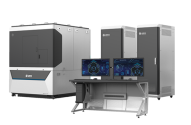
Jinjing Technology's Electron Beam Lithography System Receives First Certification for Domestic Production [TusStar Investment]
Recently, Beijing Jinjing Technology Co., Ltd., a TusStar portfolio company, officially received Beijing's first major technical equipment certification for its independently developed Pharos 310 electron beam lithography system. This marks the product as the first domestically produced commercial electron beam lithography system to receive official certification. This first-of-its-kind certification is not only a high recognition of Jinjing Technology's technological strength, but also a strong demonstration of China's independent innovation capabilities in the field of high-end scientific instrumentation.

Electron beam lithography systems, also known as electron beam lithography systems, are widely used in national strategic fields such as micro-nano processing and semiconductor device fabrication. Previously, my country had long relied on imports in this field and was repeatedly subject to embargoes, severely hampering the development of science and technology. Jinjing Technology's Pharos series of electron beam lithography systems has broken this bottleneck, providing key support for resolving the bottleneck in this field.


Electron beam lithography systems, also known as electron beam lithography systems, are widely used in national strategic fields such as micro-nano processing and semiconductor device fabrication. Previously, my country had long relied on imports in this field and was repeatedly subject to embargoes, severely hampering the development of science and technology. Jinjing Technology's Pharos series of electron beam lithography systems has broken this bottleneck, providing key support for resolving the bottleneck in this field.


No all wafers are equal. some of the wafers are 12 inch other are 8 inch, some are certified for logic manufacturing 28nm, 14nm and 7nm -others for DRAM or NAND - others power chips - others for MEMS, some wafers are polished from the Silicon Ingot cut others are grown epitaxially, other are SOI others are just doped.It's monstrous. There will be a glut of wafers.
In reality is difficult to know if they are completely self-sufficient in every type of wafers or not, my bet is that in most applications China is closer to self-sufficient in wafers than not.
As long as domestic DUV/EUV is in place, a large number of domestic chips that were previously unproduced will flood the market and consume these wafers.It's monstrous. There will be a glut of wafers.
CPU, GPU, NPU, you name it. Although Huawei has taken the lead in launching domestically produced 7nm chips, there are still a large number of companies still can't secure production slots and stuck at 12nm
