Chinese semiconductor thread II

GulfLander

Brigadier
Registered Member
Google translated
"Professor Fang Lu's team at Tsinghua University broke a century-old dilemma and successfully developed the world's first sub-angstrom-level snapshot spectral imaging chip - "Yuheng", which has overcome the long-term problem of being unable to achieve both spectral resolution and imaging speed. It is based on a revolutionary reconfigurable computational optical imaging architecture, which condenses the traditional and cumbersome physical spectroscopy system into a chip that is only 2 cm square.
Please, Log in or Register to view URLs content!

....
Please, Log in or Register to view URLs content!
....
Integrated lithium niobate photonics for sub-ångström snapshot spectroscopy
Please, Log in or Register to view URLs content!
 
Last edited:

test1979

Junior Member
Registered Member
15 companies including Xinkailai and North Huachuang jointly released the "Verification Results of the First Set of Domestic 8-inch Wide Bandgap Semiconductor Process Equipment".

Wide-bandgap semiconductors (such as silicon carbide (SiC) and gallium nitride (GaN)) are a new generation of semiconductor materials. Compared to traditional silicon-based semiconductors, they possess superior properties such as high-voltage and high-temperature resistance, and high-frequency efficiency. They are central to high-end applications such as electric vehicles, 5G communications, big data centers, new energy, and industrial motors.

The two key areas of focus are the 8-inch wafer and the localization of equipment. Currently, the mainstream SiC substrate is 6-inch. Upgrading to 8-inch wafers means more chips can be cut from a single wafer, significantly reducing costs—an inevitable trend for large-scale industrial development. However, the process equipment required to achieve this goal (such as crystal growth furnaces, epitaxial growth equipment, and etching machines) has long been monopolized by foreign giants. The successful verification of this "first set" marks a breakthrough from zero to one in China's upstream and core equipment for wide-bandgap semiconductors, breaking through foreign technological barriers.

bandaoti.jpg
 

tokenanalyst

Lieutenant General
Registered Member

Xinlian Integrated Circuit to invest 1.8 billion in 12-inch wafer fabs!​


Xinlian Integrated announced after the market today (October 16) that the company plans to apply for new policy financial instruments of no more than RMB 1.8 billion from China Development Bank's wholly-owned subsidiary, China Development Bank New Policy Financial Instrument Co., Ltd.

The announcement shows that Xinlian Integration and its holding subsidiary Xinlian Pioneer are both national high-tech enterprises. At the same time, the various chips required for power module applications manufactured and produced by the "Phase III 12-inch Integrated Circuit Digital-Analog Hybrid Chip Manufacturing Project" undertaken by Xinlian Pioneer are the foundation of many strategic emerging industries such as artificial intelligence, the Internet of Things, and new energy vehicles. They are highly consistent with the development direction of digitalization and intelligence, and accurately match the policy orientation of scientific and technological self-reliance and the development and expansion of strategic emerging industries.

Taking advantage of the opportunity of implementing and promoting new policy-based financial instruments, and in order to ensure the continued implementation of the "Phase III 12-inch Integrated Circuit Digital-Analog Hybrid Chip Manufacturing Project", Xinlian Integrated Circuit stated that it plans to apply to China Development Bank's wholly-owned subsidiary China Development Bank New Policy Financial Instrument Co., Ltd. for policy-based financial instruments of no more than RMB 1.8 billion, with a term of 5 years.

According to the announcement, in 2023, Xinlian Integrated Circuits (CI) has approved the implementation of the "Phase III 12-inch Integrated Circuit Digital-Analog Hybrid Chip Manufacturing Project" by Xinlian Pioneer. The projected total investment is RMB 22.2 billion, with a production capacity of 100,000 chips per month. These products can be widely used in new energy, automotive, industrial control, and consumer applications. The production line has completed preliminary construction, and all relevant process platforms have entered mass production.​

Please, Log in or Register to view URLs content!
 

tokenanalyst

Lieutenant General
Registered Member

Rarefied Gas Simulation in the Dynamic Gas Lock of EUV Lithography: A Comparative Study of DSMC, ESBGK, ESBGK-DSMC, and ESFP Method​


This study focuses on the dynamic gas lock (DGL) in extreme ultraviolet lithography (EUVL), comparing four rarefied gas simulation methods: DSMC, ESBGK, ESBGK–DSMC, and ESFP. For multicomponent, polyatomic gas flows under rarefied and non-equilibrium conditions, the transport coefficients in the ESBGK method were evaluated using both Wilke’s mixing rule and collision integrals. Results show that, relative to the DSMC benchmark, the ESBGK–DSMC hybrid method achieves the closest agreement, with an average deviation of 1.52% in suppression rate, while improving computational efficiency by a factor of 4.5. The standalone ESBGK(Collint) and ESBGK(Wilke) models exhibit average deviations of 3.53% and 1.79%, respectively, in suppression rate relative to the DSMC benchmark. Both, however, achieve an identical improvement in computational efficiency, being approximately 4.6 times faster than DSMC. In the ESBGK method (Collint and Wilke), the transport coefficients of the gas mixture show close agreement with benchmark values for the bulk carrier gas; however, for trace species with low molar fractions, sensitivity to collisional kinetics causes more pronounced deviations. From a temperature perspective, deviations at r1 are 0.08% for the clean gas and 0.37% for the contaminant. In contrast, the ESFP method shows major deviations in multicomponent systems, reaching 190.5%.

Please, Log in or Register to view URLs content!
 

tokenanalyst

Lieutenant General
Registered Member

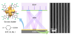
Halogenated Metal-Organic Clusters for High-Resolution Extreme Ultraviolet Lithography Resists​


The relentless drive toward miniaturization in the semiconductor industry demands photoresists capable of patterning sub-20 nm features for next-generation extreme ultraviolet (EUV) lithography. Metal-oxo clusters, with sub-5 nm molecular dimensions, structural tunability, and high EUV absorption via metal centers, have emerged as promising EUV photoresist candidates. Advancing next-generation photoresist materials necessitates resolving the inherent trade-offs between sensitivity, resolution, and line-edge roughness. In this work, we report a series of halogenated metal-organic clusters based EUVL photoresists, aiming to modulate the sensitivity, resolution, and line-edge roughness. Here, we report the synthesis of halogenated metal-organic clusters as EUVL photoresists, designed to modulate the resolution-line edge roughness-sensitivity trade-off. Sub-20 nm critical dimensions and line edge roughness below 2 nm were achieved with the clusters by EUVL. The results demonstrated that halogen elements influenced the sensitivity of the clusters. To unravel the EUV-driven reaction pathways, we analyzed the chemical transformations in these clusters after exposure using X-ray photoelectron spectroscopy and Fourier-transform infrared spectroscopy. These findings pave the way for the rational design of high-performance EUV photoresists.

1760657149487.png

Please, Log in or Register to view URLs content!
 

tokenanalyst

Lieutenant General
Registered Member

Fuga Gallium Industry: Releases new surface gallium oxide substrate products​

Fuga Gallium Industry simultaneously launched a new type of (011) crystal surface gallium oxide substrate product, covering small wafers and 2-inch standard specifications, and opened customized services for 4-inch substrates and 2-4 inch epitaxial wafers, further improving the company's gallium oxide material product system.

Product and Equipment Layout The company has independently developed several sets of key equipment and process packages:​
  • EFG equipment : The world's first EFG equipment with "one-click crystal growth" function, suitable for 2-6 inch crystal growth;​
  • VB method equipment : achieved the first breakthrough in China's 6-inch VB method single crystal growth;​
  • Grinding and polishing equipment : In view of the brittleness and easy cleavage characteristics of gallium oxide, we develop special grinding and polishing equipment for 2-6 inch substrates.​
1760658055158.png1760658134309.png
The company has currently obtained 6 domestic patents and 4 international patents, and has passed the ISO9001 quality system certification. It can provide 10mm to 6-inch polycrystalline gallium oxide substrates and MOCVD/MBE epitaxial wafer products.


Please, Log in or Register to view URLs content!
 

tphuang

General
Staff member
Super Moderator
VIP Professional
Registered Member

This probably will not surprise anyone, but the domestic lithography machine was already reported to be testing out at SMIC (by the FT article). The progress has advanced enough where it seems to me that people that are connected to Huawei (like this guy) has gotten news that YMTC is trialing their all domestic production line and that they will enter production next year. My guess is in the first half of next year. That also jives with the SiCarrier all-domestic 28nm story & ASML saying China revenue % will decline and all the other stuff.

So at this point, it seems to me that fine tuning and improving the domestic machines and scaling up production is the main challenge. By 2030, I would imagine that there is going to be very little market share for foreign SMEs.
 
Top