Chinese semiconductor thread II

vincent

Grumpy Old Man
Staff member
Moderator - World Affairs
it's 14nm or below for semiconductor production requires permit on a case by case,
Even if it contains 0.1% of Chinese rare earth or tech. I heard this was initiated by Pakistan using chinese tech and equipments to process and export rare earth to US. That and Trump 's new tariffs on Chinese ships prompts China strong new response.

If trumps slap additional 100% tariffs on all Chinese goods which becomes 155%, I think China then would bring down TSMC and that would bring down entire west tech sector.

So depending how Trump reacts the new rule.
Jesus, how many times i have to debunk this piece of shit?

Please, Log in or Register to view URLs content!

According to Sharif’s office, the partnership will immediately begin the export of “readily available minerals” – including antimony, copper, gold, tungsten and rare earth elements – from Pakistan.

The statement added that the MoU aims to spur the eventual establishment of a specialised refinery in Pakistan to produce “intermediate and finished products dedicated to meeting the rapidly growing demand of the US market”.

The MoU is not a binding mining licence, rather, analysts say, it is an early-stage instrument that signals interest.

“From the USSM’s side an MoU gives goodwill at early stage in potential projects that may come, while the broad nature of the MoU means that whatever deposits show the most potential quickest can come online quickly,” Zain Kazmi, chief operating officer of Islamabad-based Capital Strategies Group and an adviser to the Washington DC-based Critical Minerals Forum, told Al Jazeera.
 

pbd456

Junior Member
Registered Member
theoretically, but there is no evidence at this point that China will block civilian usage of rare earth components. I don't really want to speculate until there is proof for that. So, we can only say they are capable of blocking production of AI chips.
But AI are military and the big AI are all contractors for usa military. Some ai companies are declaring china is an enemy
 

Wrought

Senior Member
Registered Member
To the surprise of nobody, the US turned out to be behind the Nexperia move despite official denials from the Dutch government. Reminder that it started on September 30.


The U.S. and the Netherlands typically cooperate closely on computer chip industry export controls. A Dutch Economic Affairs Ministry spokesperson, however, said there was no U.S. involvement in its decision regarding Nexperia and the timing was "purely coincidental".

Please, Log in or Register to view URLs content!

A few days later, Nexperia's Chinese operations were put under export ban in response.

China responded almost immediately by imposing an export ban on Nexperia. Letters to customers show that the measure has been in force since October 4 and applies to products from the factory in the southern province of Guangdong. The Chinese authorities classify the chips as so-called dual-use products, which can be used for both civilian and military purposes.

The export ban is causing great concern among European customers, especially in the automotive and electronics sectors. According to the German distributor Components at Service, there are no immediate alternatives available for some parts, which could cause production processes to come to a standstill or be delayed for a long time.

Please, Log in or Register to view URLs content!
 

GulfLander

Brigadier
Registered Member
Chinese researchers develop high-precision scalable analog matrix computing chip: media report
Chinese researchers develop high-precision scalable analog matrix computing chip based on resistive memory, realizing for the first time an analog computing system whose accuracy rivals that of digital computing in accuracy, according to the Science and Technology Daily.

The breakthrough was achieved by a team led by researcher Sun Zhong from the Institute for Artificial Intelligence at Peking University, in collaboration with the School of Integrated Circuits, according to the report.

The chip delivers computing throughput and energy efficiency 100 to 1,000 times greater than current top digital processors (GPUs) in solving key scientific problems such as large-scale MIMO signal detection. The findings were published on October 13 in Nature Electronics, according to the report.

How to achieve both high precision and scalability in analog computing — allowing it to fully leverage its inherent advantages in modern computational tasks — has long been a century-old challenge for the global scientific community, according to the Science and Technology Daily.

Sun's team took an integrated innovation approach, combining novel devices, original circuits, and classical algorithms to build a high-precision, scalable analog matrix solver based on resistive memory arrays — achieving, for the first time, 24-bit fixed-point accuracy in analog computing.

In terms of performance, it outperformed a high-end GPU core when solving a 32×32 matrix, and for larger 128×128 problems, its computing throughput was more than 1,000 times faster than top digital processors — what takes a GPU a full day, this chip can finish in about a minute, according to the report.

At the same precision, it is also over 100 times more energy-efficient, offering a breakthrough for next-generation high-efficiency computing centers, according to the report.
Please, Log in or Register to view URLs content!
 

tokenanalyst

Lieutenant General
Registered Member

Total investment exceeds 37 billion yuan! A new semiconductor project in Inner Mongolia​


According to Ordos Technology, the project, with a total investment of approximately 37.2 billion yuan and a land area of approximately 1,050 mu (approximately 1,050 mu), plans to build the Inner Mongolia Semiconductor Science Park in the Mengsu Economic Development Zone. This will create a comprehensive base integrating production, learning, and research around semiconductor materials, with supporting facilities, including a research institute, employee living quarters, and commercial areas . Construction is scheduled to begin by the end of 2025, with plant and supporting facilities completed by the end of 2026 , and production to begin by the end of 2027. Upon commissioning, the project is expected to achieve an annual output of 2.4 million 12-inch wafers with a sub-30nm process. At full production, this project is expected to generate an annual output value of approximately US$42 billion and generate 15 billion yuan in tax revenue.
At the signing ceremony, Zhang Wensong, Chairman of China Construction International Industrial Investment Group, introduced the basic situation of the project and supporting needs, and expressed that he would take the signing as an opportunity to accelerate the construction of semiconductor slicing epitaxial plant, chip plant, and packaging plant to ensure the project is completed and put into production on time.

Please, Log in or Register to view URLs content!
 

tokenanalyst

Lieutenant General
Registered Member

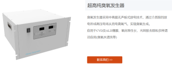
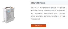
Zhihua Semiconductor Zhuhai Headquarters Base officially started production with an annual output of 1,000 sets of semiconductor ozone equipment to help domestic substitution​


The opening ceremony of the headquarters base of Zhuhai Zhihua Semiconductor Technology Co., Ltd. (hereinafter referred to as "Zhihua Semiconductor") was grandly held in Zone D of the Greater Bay Area Intelligent Manufacturing Industrial Park operated by Zhuhai Science and Technology Industry Group.

The successful establishment of Zhihua Semiconductor is the result of Zhuhai City and the High-tech Zone's continued commitment to the integrated circuit industry and the convergence of innovative elements. As a core hub in the company's strategic layout, the Zhuhai base plans a total investment of 200 million yuan. Upon completion, it is expected to produce 1,000 sets of semiconductor ozone equipment annually, with an annual output value of 1 billion yuan upon reaching full production. It will also create 300 high-quality jobs for the local area, becoming a new fulcrum for high-quality regional economic development.​

1760470421492.png1760470385893.png1760470482992.png

In the chip manufacturing process, cleaning accounts for approximately 30% of the entire process, directly determining chip yield, yet it has long been a shortcoming in domestic production. Zhihua Semiconductor, one of the few domestic companies to master the core technologies for the entire ozone equipment chain, has successfully broken the foreign monopoly through over a decade of technological advancement. Its core products, such as high-concentration ozone gas systems and high-purity ozone water systems, offer ozone gas concentrations up to 420g/m³ and ozone water concentrations consistently above 140ppm, enabling the precise removal of nanoscale impurities from wafer surfaces. These products are already in use at numerous advanced wafer fabs in Taiwan and Southeast Asia. Furthermore, the company's innovatively developed carbon dioxide functional water system offers a new, environmentally friendly and efficient solution for the industry.

Please, Log in or Register to view URLs content!
 

tokenanalyst

Lieutenant General
Registered Member

A total investment of 1 billion yuan was signed for a car-grade semiconductor project in Guangzhou and Foshan.​


According to the official WeChat account of "Nanhai Guicheng", the signing ceremony of the automotive-grade semiconductor project of Chongqing Yuntong Technology Co., Ltd. (hereinafter referred to as "Yuntong Technology") was recently held in Foshan, Guangdong, marking that this advanced domestic enterprise in the field of automotive-grade power semiconductors has officially settled in the Guicheng Wenhan Lake International Science and Technology Innovation Cooperation Zone.

The project, with a total investment of 1 billion yuan, will build the South China headquarters of Yuntong Technology and create a technology research and development base for innovative packaging products of dedicated integrated circuit chips and devices, injecting strong "core" power into the development of strategic emerging industries in Foshan and even the Guangdong-Hong Kong-Macao Greater Bay Area.
According to information, Yuntong Technology was established in 2018. It is a semiconductor Fablite (light wafer factory) company based on motor drive and power inverter scenarios, with the ability to output application technology solutions, providing automotive-grade power semiconductors and ASIC chips, products, modules, and independent control of the entire chain.

As of June 2025, Yuntong Technology has applied for 301 intellectual property rights, 140 of which have been granted, demonstrating strong innovation capabilities. It has delivered over 400 million chips and maintained a record of "zero quality incidents."
In the future, Yuntong Technology's South China headquarters will focus on the research and development and mass production of four major characteristic packaging series module products and board-level solutions in the fields of new energy vehicles, drones, robots and power systems.

Please, Log in or Register to view URLs content!
 

tokenanalyst

Lieutenant General
Registered Member

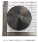
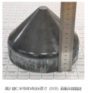
GaRen Semiconductor first uses of the VB method to grow the thickest 6-inch (010) surface gallium oxide crystal.​

Hangzhou Gallium Ren Semiconductor Co., Ltd. (hereinafter referred to as "Gallium Ren Semiconductor") once again achieved breakthrough results in crystal growth technology. Based on the independently developed gallium oxide dedicated crystal growth equipment, it successfully achieved 6-inch (010) surface gallium oxide crystal growth using the vertical Bridgman method (VB method), and the equal diameter section length exceeded 40mm, reaching the international leading level.

1760473277288.png1760473298483.png

Advantages of Gallium Oxide Growth on (010) Surfaces

Among the common mainstream crystal planes of gallium oxide single crystal substrates, the (010) substrate has excellent performance in physical properties and epitaxy:

1. (010) The substrate has the highest thermal conductivity, which is beneficial to improving the performance of power devices;
2. The (010) substrate has a faster epitaxial growth rate and good epitaxial matching, making it the preferred crystal plane for epitaxy.

At present, Gallium Ren Semiconductor has launched a number of wafer-level (010) gallium oxide single crystal substrate products. These products are aimed at the scientific research market, meeting the demand for (010) substrates in the scientific research field and promoting collaborative cooperation between industry, academia and research.

Gallium speed of the Gallium Core VB method

In September 2024, Gallium Ren Semiconductor launched its independently developed dedicated gallium oxide crystal growth equipment, which not only meets the high temperature and high oxygen environment required for gallium oxide growth, but also can perform fully automated crystal growth, reducing manual intervention and significantly improving production efficiency and crystal quality.
1760473325957.png

Please, Log in or Register to view URLs content!
 
Top