
You are using an out of date browser. It may not display this or other websites correctly.
You should upgrade or use an alternative browser.
You should upgrade or use an alternative browser.
Chinese semiconductor industry
- Thread starter Hendrik_2000
- Start date
- Status
- Not open for further replies.


sr, only Chinese..
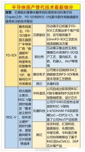
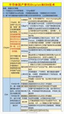
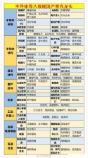
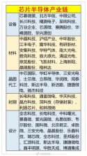
A complete list of domestic alternatives to semiconductors Including EDA, and the integration of the latest technology Chiplet, FD-SOI and RISC-V
A complete list of domestic alternatives to semiconductors Including EDA, and the integration of the latest technology Chiplet, FD-SOI and RISC-V
Attachments
-
 cfb0cc7dgy1h5015nrn2ej20ow18a7ih.jpg178.1 KB · Views: 65
 -
 cfb0cc7dgy1h5015k05etj20u01hgki6.jpg219.7 KB · Views: 52
 -
 cfb0cc7dgy1h5015n2zxbj20u01hgqtv.jpg219.7 KB · Views: 40
 -
 cfb0cc7dgy1h5015lzwn8j20lm12iqd1.jpg161.6 KB · Views: 39
 -
 cfb0cc7dgy1h5015le1u8j20tz1hstuk.jpg188.6 KB · Views: 39
 -
 cfb0cc7dgy1h5015kikupj20jg0yoqcb.jpg175.4 KB · Views: 47
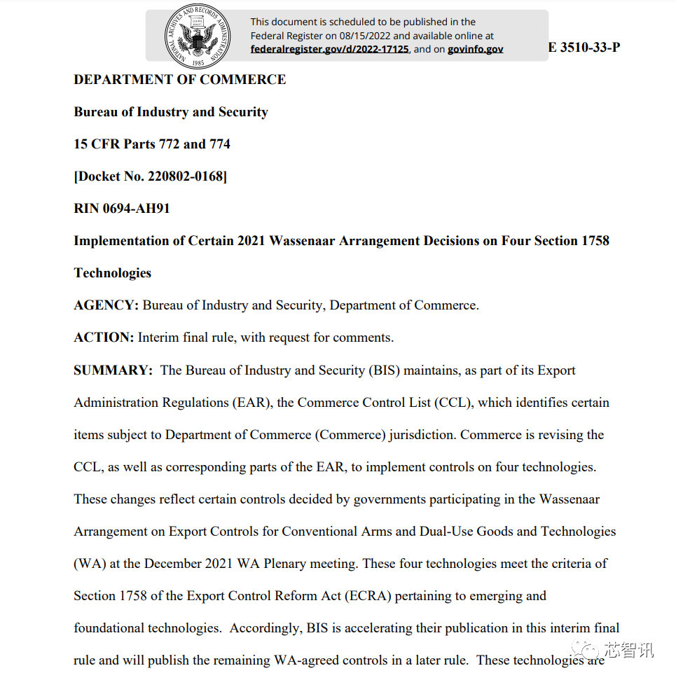
The United States imposes a new export ban on China: involving four technologies including EDA, gallium oxide and diamond materials
On August 12, local time, the U.S. Department of Commerce’s Bureau of Industry and Security (BIS) disclosed a new interim final rule on export restrictions in the Federal Register, involving advanced semiconductors, turbine engines and other fields.
The ban applies to EDA/ECAD software necessary for integrated circuits with a GAAFET (Around Gate Field Effect Transistor) structure, ultra-wide bandgap semiconductor materials represented by diamond and gallium oxide, pressure gain combustion (PGC) Four technologies implemented new export controls.
GAAFET related EDA software
EDA/ECAD refers to electronic computer aided software used to design, analyze, optimize and verify the performance of integrated circuits or printed circuit boards. As early as August 3, Xinzhixun reported that "the United States will cut off the supply of EDA tools related to GAAFET technology to China". The announcement of the ban further confirms the news.
As the successor of FinFET, GAAFET is considered to be the key technology for mass production of 3nm and below semiconductor process technology. At the end of June this year, Samsung has announced the first mass production of the 3nm process based on GAAFET technology. The 3nm that TSMC is currently mass-producing is still based on FinFET technology, and it is expected to introduce GAAFET technology at 2nm.
In other words, the US ban will limit the export of EDA software to China that can be used in chip designs for advanced semiconductor processes of 3nm and below. This move will limit the breakthrough of Chinese chip designers to advanced processes of 3nm and below.
BIS is also currently soliciting public comments to determine which specific features of ECAD are particularly useful in designing GaAs FET circuits to ensure that the U.S. government can effectively enforce the regulation.
Related article "It is rumored that the United States will cut off the supply of GAA technology-related EDA tools to China"
Gallium oxide and diamond
As for the wide bandgap semiconductor materials gallium oxide (Ga2O3) and diamond (including silicon carbide SiC): gallium nitride and silicon carbide are the main materials for the production of complex microwave, millimeter wave devices or high power semiconductor devices, with the potential to create more complex devices , can withstand higher voltage or temperature.
At present, compound semiconductors represented by silicon carbide and gallium nitride have received a lot of attention, and they will play a role that traditional silicon devices cannot achieve in future high-power, high-temperature, and high-voltage applications. Especially in the automotive field, one of the three emerging application fields (automotive, 5G and the Internet of Things) in the future, there will be very broad development prospects. However, gallium oxide has a wider band gap than silicon carbide and gallium nitride, which makes this compound semiconductor unique in higher power applications.
Gallium oxide is a wide-bandgap semiconductor with a band gap of EG=4.9eV, far exceeding that of silicon carbide (about 3.4eV), gallium nitride (about 3.3eV) and silicon (1.1eV), and its electrical conductivity and luminescence characteristics are good. Therefore, it has broad application prospects in optoelectronic devices and high-power scenarios. Although, the mobility and thermal conductivity of gallium oxide are low, especially the thermal conductivity is its main short board. However, relatively speaking, these disadvantages do not have much impact on the characteristics of power devices, because the performance of power devices mainly depends on the breakdown electric field strength.
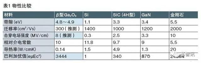
△Ga2O3 has five main crystal forms: α, β, γ, δ, and ε. Among them, the β structure is the most stable, and most of the research reports related to the crystal growth and physical properties of Ga2O3 use the β structure. The breakdown electric field strength of β-Ga2O3 is about 8MV/cm, which is more than 20 times that of Si and more than twice that of SiC and GaN.
Compared with silicon materials, gallium nitride, silicon carbide, etc., the forbidden band width of diamond semiconductor materials is as high as 5.45 eV, and the biggest advantage lies in higher carrier mobility (holes: 3800 cm2V-1s-1, electrons: 4500 cm 2V-1s-1), higher breakdown electric field (>10 MVcm-1), greater thermal conductivity (22 WK-1cm-1), its intrinsic material advantage is the highest thermal conductivity in nature It can meet the needs of high power, strong electric field and radiation resistance in the future, and is an ideal material for making power semiconductor devices. It has broad application prospects in smart grid, rail transit and other fields.
However, according to Li Chengming, a professor at the Institute of New Materials Technology at the University of Science and Technology Beijing, there is still a long way to go for diamond to achieve commercial applications. The high cost and small size of diamond materials are the main obstacles restricting the development of diamond power electronics. For example, the dislocation density of nitrogen-doped diamond single crystal flakes (6 mm × 7 mm) in CVD production can currently be as low as 400 cm-2; The dislocation density is still up to the order of nearly 107 cm-2, and the high defect density remains a challenge.
pressure gain burn
Pressure Gain Combustion (PGC) is a technology that has the potential to increase the efficiency of gas turbine engines by more than 10 percent, potentially impacting aerospace, rocket and hypersonic missile systems. PGC technology utilizes a variety of physical phenomena, including resonant pulse combustion, constant volume combustion, and knocking, to create effective pressure in the combustion chamber while consuming the same amount of combustion.
BIS is currently unable to confirm whether any of the engines in production use the technology, but there has been plenty of research pointing to potential production.
So while Chinese materials providers will have market access to the entire world, including the United States, Americans material providers market access will be limited by the goverment to a few countries. Then when Chinese providers become the dominant players, they will blame China policies instead of themselves, rinse and repeat.
A major breakthrough! Jingsheng Electromechanical successfully developed an 8-inch N-type SiC crystal
After more than half a year of technical research by the R&D team of the crystal laboratory, the first 8-inch N-type SiC crystal was successfully released on August 12, and the research and development of the third-generation semiconductor material SiC of Jingsheng has entered the 8-inch era. Another landmark achievement in the field of wide-bandgap semiconductors.

Silicon carbide devices have the advantages of high temperature resistance, high pressure resistance, good high frequency characteristics, high conversion efficiency, small size and light weight, and are widely used in new energy vehicles, rail transit, photovoltaics, 5G communications and other fields. However, silicon carbide with "high hardness, high brittleness and low fracture toughness" has extremely strict requirements on the production process, and the preparation of large-sized silicon carbide crystals has always been the "neck" technology of the industry.
The 8-inch SiC crystal successfully developed this time has a thickness of 25mm and a diameter of 214mm, which is a major breakthrough for Jingsheng in the research and development of large-size SiC crystals. It not only successfully solved the difficult problems of uneven temperature field, crystal cracking, and gas-phase raw material distribution during the growth of 8-inch SiC crystals, but also solved the problem that the substrate accounted for too much in the cost of SiC devices, which is widely used for large-size SiC substrates. lay the foundation.
The independent and controllable SiC crystal growth and processing technology is the key to seizing the commanding heights of future competition! For a long time, Jingsheng Electromechanical has always adhered to the original mission of "building a leading enterprise in semiconductor material equipment and developing a green and intelligent high-tech manufacturing industry", and has continuously extended its product series through self-developed equipment, thermal fields and process technology. Since 2017, the silicon carbide business has been laid out. By 2020, the crystal growth and processing pilot line will be established. The diameter of the SiC crystal has also increased from the original 4 inches to the current 8 inches, further narrowing the technological gap at home and abroad and ensuring my country's silicon carbide industry. Autonomous and controllable in key core technologies.

Scientific and technological innovation, responsible for the country! The successful development of the 8-inch SiC conductive single crystal has not only greatly enhanced the international competitiveness of Jingsheng in the SiC single crystal substrate industry, but also contributed to the development of the localization of the wide bandgap semiconductor industry. Big gift!
Silicon carbide devices have the advantages of high temperature resistance, high pressure resistance, good high frequency characteristics, high conversion efficiency, small size and light weight, and are widely used in new energy vehicles, rail transit, photovoltaics, 5G communications and other fields. However, silicon carbide with "high hardness, high brittleness and low fracture toughness" has extremely strict requirements on the production process, and the preparation of large-sized silicon carbide crystals has always been the "neck" technology of the industry.
The 8-inch SiC crystal successfully developed this time has a thickness of 25mm and a diameter of 214mm, which is a major breakthrough for Jingsheng in the research and development of large-size SiC crystals. It not only successfully solved the difficult problems of uneven temperature field, crystal cracking, and gas-phase raw material distribution during the growth of 8-inch SiC crystals, but also solved the problem that the substrate accounted for too much in the cost of SiC devices, which is widely used for large-size SiC substrates. lay the foundation.
The independent and controllable SiC crystal growth and processing technology is the key to seizing the commanding heights of future competition! For a long time, Jingsheng Electromechanical has always adhered to the original mission of "building a leading enterprise in semiconductor material equipment and developing a green and intelligent high-tech manufacturing industry", and has continuously extended its product series through self-developed equipment, thermal fields and process technology. Since 2017, the silicon carbide business has been laid out. By 2020, the crystal growth and processing pilot line will be established. The diameter of the SiC crystal has also increased from the original 4 inches to the current 8 inches, further narrowing the technological gap at home and abroad and ensuring my country's silicon carbide industry. Autonomous and controllable in key core technologies.
Scientific and technological innovation, responsible for the country! The successful development of the 8-inch SiC conductive single crystal has not only greatly enhanced the international competitiveness of Jingsheng in the SiC single crystal substrate industry, but also contributed to the development of the localization of the wide bandgap semiconductor industry. Big gift!
If we want to break through the most advanced DUV lithography machine, we can see from the name that the difficulty lies in the infiltration technology, which is one of the most critical reasons why our domestic lithography machine cannot break through 28 nanometers for a long time. However, recently, our domestic related company, Chier Electromechanical, has made relevant breakthroughs in lithography machine infiltration technology. In the high-end integrated semiconductor industry, it has also successfully iterated to the eighth generation, realizing high-precision control of liquid during infiltration. , which can be controlled to an error of 0.001 degrees, which is quite difficult.
And the related lithography machine research and development experimental base has also started mid-term testing and trial production. In other words, the development of DUV lithography machines is basically no problem, and the focus will be on yield and productivity in the future. Coupled with the technological breakthroughs made by Guowang Optical in the exposure system and lens provision of lithography machines some time ago, it can be said that the main technical difficulties in immersion lithography machines have been basically broken through.
In mid-April 2022, Professor Zhu Yu of Tsinghua University led the team and released public news, saying that with the joint breakthrough of the team and Huazhuo Jingke, the self-developed dual-stage lithography machine was successfully developed. The latter It is the top supplier of core components of lithography machines in China, and it can be regarded as breaking ASML's monopoly in the field of dual-stage lithography machines, becoming the second company and team in the world with this technology.
Huahai Qingke: There are multiple machines on the client side for parallel verification of different 14nm processes
On August 8, Huahai Qingke Co., Ltd. (hereinafter referred to as "Huahai Qingke") stated on the investor platform that the company has multiple machines on the client side for parallel verification of different 14nm processes, and it is progressing smoothly. There are differences in the proportion of advance receipts agreed upon by different customer orders. The equipment industry usually charges 30% of advance receipts for orders signed.
It is reported that Huahai Qingke, established in 2013, is a high-end semiconductor equipment manufacturer with core independent intellectual property rights, mainly engaged in the research and development, production, sales of chemical mechanical polishing (CMP), grinding and other equipment and supporting consumables, as well as wafer regeneration OEM service. The company's CMP equipment series products have been widely used in batches of well-known integrated circuit production lines at home and abroad, and the CMP equipment produced can be widely used in 12-inch and 8-inch integrated circuit production lines.
On June 8, Huahai Qingke was listed on the Science and Technology Innovation Board of the Shanghai Stock Exchange.
In addition, on August 1, Huahai Qingke won the bid for one chemical mechanical polishing machine for the chemical mechanical polishing machine project of Shenzhen Huixin Communication Technology Co., Ltd.
Bro remember @Pkp88 post about A-SET and it specifically mentioned Qier Electromechanical way back in 2020, so we may assume that the tech development was finished in 2018 or 2019 and the verification was deemed a success in 2021.If we want to break through the most advanced DUV lithography machine, we can see from the name that the difficulty lies in the infiltration technology, which is one of the most critical reasons why our domestic lithography machine cannot break through 28 nanometers for a long time. However, recently, our domestic related company, Chier Electromechanical, has made relevant breakthroughs in lithography machine infiltration technology. In the high-end integrated semiconductor industry, it has also successfully iterated to the eighth generation, realizing high-precision control of liquid during infiltration. , which can be controlled to an error of 0.001 degrees, which is quite difficult.
And the related lithography machine research and development experimental base has also started mid-term testing and trial production. In other words, the development of DUV lithography machines is basically no problem, and the focus will be on yield and productivity in the future. Coupled with the technological breakthroughs made by Guowang Optical in the exposure system and lens provision of lithography machines some time ago, it can be said that the main technical difficulties in immersion lithography machines have been basically broken through.
In mid-April 2022, Professor Zhu Yu of Tsinghua University led the team and released public news, saying that with the joint breakthrough of the team and Huazhuo Jingke, the self-developed dual-stage lithography machine was successfully developed. The latter It is the top supplier of core components of lithography machines in China, and it can be regarded as breaking ASML's monopoly in the field of dual-stage lithography machines, becoming the second company and team in the world with this technology.
Pkp88
New Member
Registered MemberThere have been some online posts about SMEE capabilities. Below I have posted the translated text and links to actual site. I would be curious what people think of this information.
Attachments
-

Image1.PNG
152.3 KB · Views: 111 -

Image2.PNG
195.3 KB · Views: 24
Salty Article coming from Bloomberg, we all know that SMIC doesn't produce leading edge node like 5nm and even 7 nm chips for Smartphone so what the fuzz about, why focus on them rather than TSMC, Intel and Samsung. To be honest they had a point BUT exaggerating it doesn't help.
Bloomberg News
Fri, August 12, 2022 at 11:12 AM·3 min read

In this article:
(Bloomberg) -- Semiconductor Manufacturing International Corp. warned that clients in sectors such as smartphones were freezing orders, underscoring how a downturn in consumer electronics demand is hurting the chip sector.
Most Read from Bloomberg
Waning demand from makers of smartphones and TV components is forcing SMIC to readjust its manufacturing plans, co-CEO Zhao Haijun told analysts on Friday. The economic downturn and inventory adjustments have spurred “rapid freeze and urgent order halts” as some clients hold off on placing new orders, he said on a conference call. SMIC fell as much as 3.1% in Hong Kong.
Investors fear the notoriously cyclical chip industry is hurtling toward a prolonged slump after years of shortages led to heavy investments in capacity. SMIC is among a raft of semiconductor manufacturers now grappling with rapidly crumbling global electronics demand, as consumers leave a pandemic-era boom behind. It’s also contending with steadily tightening US export restrictions as Washington tries to contain Beijing’s technological rise.
China’s largest chipmaker reported revenue rose 42% to $1.9 billion in the second quarter, generally in line with expectations. It posted net income of $514.3 million in the second quarter, surpassing the $469.5 million average estimate.
Read more: Apple Expects to Sustain IPhone Sales in 2022 as Market Slows
What Bloomberg Intelligence Says
Semiconductor Manufacturing International’s return on equity is on track to hit a new high in 2022 despite disruptions to production and capacity expansions due to stricter US export-licensing requirements and China’s Covid-19 lockdowns. The company’s chip foundries will run at high utilization rates over the next two years amid a rapid increase in local fabless chipmaker numbers and increasing silicon content in consumer appliances and automobiles. Its shift toward higher-margin specialty chips -- less exposed to sanctions risk -- may help to offset soaring depreciation and staff costs.
- Charles Shum, analyst
Click here for the research.
Read more: China Graft Probes Stem From Anger Over Failed Chip Plans
SMIC is at the vanguard of China’s long-term ambition to produce chips sophisticated enough to replace American silicon, which comprise the majority of the country’s annual $155 billion in semiconductor consumption.
It remains a technological leader in a giant domestic industry now gripped by a series of corruption probes, as senior officials frustrated with the nation’s lack of progress in semiconductors begin to hold executives accountable. The outcome of the widening dragnet and its impact on local players remain unclear.
US sanctions have played a central role in curbing the country’s chip ambitions. The Trump administration blacklisted SMIC about two years ago on national security concerns, citing the company’s ties with the Chinese military, an allegation the chipmaker has denied. Washington is now also pressing allies into the effort, so that key suppliers like the Netherlands’ ASML Holding NV and Japan’s Nikon Corp. join its technology blockade.
Read more: US Pushes for ASML to Stop Selling Chipmaking Gear to China
In response, homegrown firms have attempted to develop alternatives to American silicon. The Shanghai-based contract chipmaker has succeeded in advancing its production technology two generations this year to 7-nanometers, though industry experts caution that may not be based on the same standards employed by far larger rivals like Taiwan Semiconductor Manufacturing Co.
SMIC has said sanctions hurt its ability to develop more sophisticated technologies. The company’s capability is severely curbed by its lack of access for instance to ASML Holding NV’s extreme ultraviolet lithography systems, which are required to make the most advanced chips.
The company said in a separate filing that Tudor Brown, the former president of Arm Ltd., has resigned from the board, confirming an earlier Bloomberg report. Zhao also resigned as an executive director, according to the company.
China’s SMIC Warns of ‘Rapid Freeze’ as Smartphone Demand Skids
Bloomberg News
Fri, August 12, 2022 at 11:12 AM·3 min read
In this article:
(Bloomberg) -- Semiconductor Manufacturing International Corp. warned that clients in sectors such as smartphones were freezing orders, underscoring how a downturn in consumer electronics demand is hurting the chip sector.
Most Read from Bloomberg
Waning demand from makers of smartphones and TV components is forcing SMIC to readjust its manufacturing plans, co-CEO Zhao Haijun told analysts on Friday. The economic downturn and inventory adjustments have spurred “rapid freeze and urgent order halts” as some clients hold off on placing new orders, he said on a conference call. SMIC fell as much as 3.1% in Hong Kong.
Investors fear the notoriously cyclical chip industry is hurtling toward a prolonged slump after years of shortages led to heavy investments in capacity. SMIC is among a raft of semiconductor manufacturers now grappling with rapidly crumbling global electronics demand, as consumers leave a pandemic-era boom behind. It’s also contending with steadily tightening US export restrictions as Washington tries to contain Beijing’s technological rise.
China’s largest chipmaker reported revenue rose 42% to $1.9 billion in the second quarter, generally in line with expectations. It posted net income of $514.3 million in the second quarter, surpassing the $469.5 million average estimate.
Read more: Apple Expects to Sustain IPhone Sales in 2022 as Market Slows
What Bloomberg Intelligence Says
Semiconductor Manufacturing International’s return on equity is on track to hit a new high in 2022 despite disruptions to production and capacity expansions due to stricter US export-licensing requirements and China’s Covid-19 lockdowns. The company’s chip foundries will run at high utilization rates over the next two years amid a rapid increase in local fabless chipmaker numbers and increasing silicon content in consumer appliances and automobiles. Its shift toward higher-margin specialty chips -- less exposed to sanctions risk -- may help to offset soaring depreciation and staff costs.
- Charles Shum, analyst
Click here for the research.
Read more: China Graft Probes Stem From Anger Over Failed Chip Plans
SMIC is at the vanguard of China’s long-term ambition to produce chips sophisticated enough to replace American silicon, which comprise the majority of the country’s annual $155 billion in semiconductor consumption.
It remains a technological leader in a giant domestic industry now gripped by a series of corruption probes, as senior officials frustrated with the nation’s lack of progress in semiconductors begin to hold executives accountable. The outcome of the widening dragnet and its impact on local players remain unclear.
US sanctions have played a central role in curbing the country’s chip ambitions. The Trump administration blacklisted SMIC about two years ago on national security concerns, citing the company’s ties with the Chinese military, an allegation the chipmaker has denied. Washington is now also pressing allies into the effort, so that key suppliers like the Netherlands’ ASML Holding NV and Japan’s Nikon Corp. join its technology blockade.
Read more: US Pushes for ASML to Stop Selling Chipmaking Gear to China
In response, homegrown firms have attempted to develop alternatives to American silicon. The Shanghai-based contract chipmaker has succeeded in advancing its production technology two generations this year to 7-nanometers, though industry experts caution that may not be based on the same standards employed by far larger rivals like Taiwan Semiconductor Manufacturing Co.
SMIC has said sanctions hurt its ability to develop more sophisticated technologies. The company’s capability is severely curbed by its lack of access for instance to ASML Holding NV’s extreme ultraviolet lithography systems, which are required to make the most advanced chips.
The company said in a separate filing that Tudor Brown, the former president of Arm Ltd., has resigned from the board, confirming an earlier Bloomberg report. Zhao also resigned as an executive director, according to the company.
- Status
- Not open for further replies.