You are using an out of date browser. It may not display this or other websites correctly.
You should upgrade or use an alternative browser.
You should upgrade or use an alternative browser.
Chinese semiconductor industry
- Thread starter Hendrik_2000
- Start date
- Status
- Not open for further replies.
coolieno99
Junior Member
Google translation for above olalavn post on EUV lithography :
Conductor discloses patent for exposure imaging structure, reflective photomask set and projection lithography machine for EUV lithography
The website of the State Intellectual Property Office recently published the invention patent application of Shanghai Chuanxin Semiconductor Co., Ltd. "exposure imaging structure, reflective photomask set and projection lithography machine".
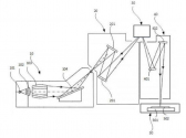
According to the patent specification, the invention provides an exposure imaging structure, a reflective photomask set and a projection lithography machine for EUV lithography. The exposure imaging structure includes a first reflective photomask and a second reflective photomask The stencil, after the exposure light passes through the first reflective photomask, the reflected light with the graphic information of the first reflective photomask is reflected to the second reflective photomask by the reflective device, so that the second reflective photomask is emitted from the second reflective photomask. The light reflected by the reticle simultaneously includes a combined projection pattern of the first reflective mask pattern and the second reflective mask pattern, so as to realize one-time exposure on the wafer through the combined projection pattern.
Since the first reflective mask pattern is physically separated from the second reflective mask pattern, this patented exposure imaging structure can make the edges of adjacent mask patterns free from light interaction (such as scattering, reflection or surface plasmon effects). SPP, etc.), can effectively eliminate the pattern defects on the wafer caused by the adjacent patterns, the resolution and contrast of the lithography process are greatly improved, and the pattern defects on the wafer (such as rounded corners, critical dimension (CD)) are reduced and end shrinking, etc.) are significantly improved, and a complete pattern can be obtained on the wafer with a single exposure, and the lithography process is also simplified.
, the examples given in the specification show that the light source structure comprises a plasma light source, generated from a gas or vapor, such as xenon gas, lithium vapor or tin vapor, bombarded by a carbon dioxide laser with a power of 30 kW twice per second to bombard the atomized tin (Sn) metal droplets (in which, tin metal droplets are ejected from the nozzle at a speed of 50,000 drops per second), tin (Sn) is evaporated into plasma, and the 13.5nm wavelength is obtained through the transition between high-valent tin ion energy levels of EUV light. (Proofreading / Chen Xinghua)

2022 NAND – Process Technology Comparison, China’s YMTC Shipping Densest NAND, Chips 4 Alliance, Long-term Financial Outlook
NAND is a market with fierce competition and a relentless march of progress. The number of bits of NAND manufactured and shipped has grown at a pace of 30% to 35% every year, doubling every 2 to 3 years. The initial take would be that this requires a large amount of capital dedicated to new equipment, but the NAND industry has only spent from $15B to $20B on wafer fabrication equipment every year from 2017 to 2022 despite exponential growth. The cost to produce NAND has fallen rapidly.

Similar cost scaling improvements were common decades ago in other semiconductor technologies such as DRAM and logic, but these sub-industries would consider this rate of improvement alien in the post-Moore’s Law universe. Productivity increases have been primarily driven by improvements in Lam Research’s etch and deposition tools, and the process nodes manufacturers developed.
Historically, when the semiconductor industry has held such rapid innovation, many firms were left in the dust technologically. Industry consolidation occurred. Only a few strong players emerged. 3D NAND is in a similar place today, and the future economics of the industry are in flux. Intel sold their NAND business, and there is a large amount of turmoil at Kioxia and Western Digital.
In this report, we want to conduct a status check on process technology from Samsung, SK Hynix, Micron, Solidigm, YMTC, Western Digital, and Kioxia. The quick summary is that Micron, SK Hynix, and YMTC are racing ahead of the others. At the same time, Samsung has oddly fallen behind despite being the absolute leader in NAND technology just a few years ago. and compiled the table below. It has many nuances which will be explained in the report.

The biggest highlight is that China’s YMTC is now shipping the highest density 3D NAND. We are exclusively detailing specifications and details associated with YMTC’s newest process technology which they have intentionally been concealing in 1st party materials. This is similar to . We also have information on potential sanctions/tool ban, the Chips 4 Alliance, and existing NAND fabs from SK Hynix and Samsung in China.
Lastly, we will also detail the NAND industry’s financial prospects, including the long-term through-cycle profitability and free cash flow margins. This includes discussing the shaky future of Western Digital and Kioxia in the NAND business and a rumored buyout offer.
Potential China Tool Bans, Chips 4 Alliance, Existing Fabs In China
Before we move on to the technology and business section, we want to discuss the geopolitical happenings. There have been numerous reports about the US looking to ban 3D NAND tools from China. Last year, we wrote a report for a PAC which was distributed around Washington that floated the idea and its impacts. The basic story is that Lam Research and other semiconductor manufacturing equipment firms could have tools blocked from being exported to China. If these tools were blocked, it would stop the current 3D NAND expansions by YMTC as well as Samsung and SK Hynix.The Chips 4 alliance is a potential alliance between the US, Japan, Taiwan, and South Korea. These 4 countries encompass the majority market share in every facet of the semiconductor supply chain. This includes supply chain inputs such as wafer substrates, photoresist, CMP slurry, and etchant gas. These nations also represent most wafer fabrication equipment, memory companies, foundries, and IDMs.
The alliance’s goal is to increase supply chain security; cooperate on research and development; and workforce development. The clear undertone is that this alliance will be used to contain China’s rapid rise in the semiconductor industry. South Korea is publicly being tepid about joining the alliance. Our understanding is that the South Korean administration and the public have swung to being very hawkish against China, so this could just be posturing.
If South Korea elects not to join the Chips 4 alliance, we are hearing the US may even try to force their hand. This could be achieved by banning the shipment of 3D NAND tools to China. Samsung and SK Hynix both have NAND fabs in China. Alongside YMTC’s capacity, our data shows that China totals 24% of global NAND production in Q3 2022. Furthermore, SK Hynix also has DRAM fabs in China. The US tool ban would effectively force South Korea to cooperate less with China on semiconductors as those fabs cannot be expanded.
SK Hynix is in a very tough place. They were wooed into China with significant subsidies for DRAM and NAND fabs, but now they face difficulties upgrading production. Memory relies on utilizing the latest technology to produce at the lowest cost per bit. With DRAM, SK Hynix’s latest DRAM node uses EUV lithography, which China cannot import. This means their DRAM fab will slowly fall behind. In a few years, it would be uncompetitive in cost per bit manufactured compared to SK Hynix fabs outside of China. SK Hynix has plans to convert the existing DRAM fab to 3D NAND in the future as 3D NAND tools currently have no export controls. This would be a costly capital transition, but one that has been planned for and expected for years. These plans all change if the 3D NAND tool ban occurs.
Both Samsung and SK Hynix will be in a very tough place if they cannot import 3D NAND tools into China. They could reconfigure existing facilities for new nodes, but a large portion of the productivity improvements in 3D NAND manufacturing have come from new or upgraded tools from Lam Research. Banning 3D NAND tools from China would sink YMTC’s future expansions and make it costly for Samsung and SK Hynix to continue their operations in China over the long term. If the US follows through on this ban, it could give Samsung and SK Hynix subsidies in the US to temper the blow.
YMTC
YMTC has been very coy with their new generation of NAND, marketed as Xtacking 3.0. They will not officially say the layer counts anywhere. The official line does not go beyond marketing Xtacking 3.0 as the industry’s densest 1Tb TLC NAND. We imagine YMTC wants to hide this technical detail because they fear US sanctions. Many allegories can be drawn to . It makes sense that YMTC is being coy in that context.YMTC has developed some stellar process technology. SemiAnalysis can exclusively detail specifications that YMTC did not publish. First, Xtacking 3.0 is the densest commercial 1Tb TLC NAND at 15.2Gbit/mm2. Second, an employee told us it is “more than 230-layers”; we believe 232-layers. Third, it is comparable to Micron’s 232-layer NAND in performance, utilizing a similar 6-plane architecture with a 2.4Gbps data rate. Lastly, it is already shipping to partners.

We established these facts by measuring a physical die with the virtual help of . Having access to the physical die also allowed us to confirm that it is 6-planes. We also further details by talking to employees on and off the record. We spent so much time with them at the booth that they even asked us to take the company photo. We found their new NAND packaged in SSDs at a 3rd party Taiwanese company’s booth. They were happy to tell us some other details, including shipment timing.
In the future, we may do an entire piece on their innovative technologies such as hybrid bonding CMOS over array, center driver XDEC, and the transition from Front Side Deep Trench process to a Back Side Source Connect (BSSC). YMTC also has plans to implement further logic for in-memory processing, including neuromorphic type computing with their stacked CMOS technology.

YMTC is not just a copycat with trailing edge technology like many erroneously perceive Chinese semiconductor companies on the leading edge. They are building their own innovative and unique product. While they rely heavily on the over 24 billion dollars of government subsidies, process tools from Lam Research, and licenses of critical technology from Adeia (Xperi), they are running ahead of other players in NAND with homegrown innovation.
YMTC is still behind on yields, but they have been rapidly improving them. In a couple of years, we have no doubt that YMTC will be cost competitive with even the best in the industry. They will structurally change the NAND industry. Firms that do not possess a durable advantage in technology or large subsidies will face an . YMTC’s 2nd fab is nearly full of tools, and the 3rd fab is under construction. Funding for the 4th fab is allegedly underway with construction starting as early as the middle of next year. Each of YMTC’s fabs will have 100,000 wafers per month output.
No, it doesn't.The report did mention that YMTC needs critical technology from Adeia (Xperi), an American firm that license 3D IC related IP.
No, it doesn't.
Didn't see this paragraph?
YMTC is not just a copycat with trailing edge technology like many erroneously perceive Chinese semiconductor companies on the leading edge. They are building their own innovative and unique product. While they rely heavily on the over 24 billion dollars of government subsidies, process tools from Lam Research, and licenses of critical technology from Adeia (Xperi), they are running ahead of other players in NAND with homegrown innovation.
I saw thisDidn't see this paragraph?
YMTC is not just a copycat with trailing edge technology like many erroneously perceive Chinese semiconductor companies on the leading edge. They are building their own innovative and unique product. While they rely heavily on the over 24 billion dollars of government subsidies, process tools from Lam Research, and licenses of critical technology from Adeia (Xperi), they are running ahead of other players in NAND with homegrown innovation.
Dylan Patel
Looks like is more about lawyers than "critical technology". They pay a patent troll to avoid the inconvenience of getting sue.Didn't see this paragraph?
YMTC is not just a copycat with trailing edge technology like many erroneously perceive Chinese semiconductor companies on the leading edge. They are building their own innovative and unique product. While they rely heavily on the over 24 billion dollars of government subsidies, process tools from Lam Research, and licenses of critical technology from Adeia (Xperi), they are running ahead of other players in NAND with homegrown innovation.
- Status
- Not open for further replies.


