Chinese semiconductor industry

Status
Not open for further replies.

european_guy

Junior Member
Registered Member
AMEC CEO presentation

Presentation from Dr. Yin Zhiyao, Chairman and General Manager of China Micro Semiconductor Equipment
Please, Log in or Register to view URLs content!


91cba44bd11373f06a4322aee20f4bfbfbed040f.jpg

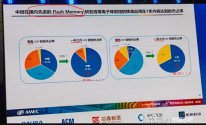
The yellow part in the picture is Northern Huachuang, which specializes in ICP etching equipment, and China Micro is CCP etching equipment, The red share in the picture should be lam research


Below text is from article author, not from the CEO:

What does it mean? It shows that since the United States imposed the strongest sanctions at the end of last year, Yangtze Storage has experienced a brief period of chaos (the second phase of expansion was suspended at the beginning of this year and some employees newly recruited for the second phase of expansion were laid off), but now it has overcome the difficulties with the help of China Micro. , start super large-scale domestic substitution!

2023 is the year of destruction of the old world of Yangtze River Storage, and it is also the year of the establishment of a new world, a key year to get rid of dependence on Western equipment. This is why the CEO of Yangtze Storage asked Western equipment vendors to buy back equipment.
 

tokenanalyst

Brigadier
Registered Member

Focuslight Technology’s laser-assisted bonding is expected to receive small batch orders​


Focuslight Technology has made breakthrough progress in LAB laser-assisted bonding applications and received prototype orders from advanced packaging customers in China and South Korea. It is expected to receive small batch orders in the second half of the year. The company has completed the development of new products for high-precision variable light spot systems used in chip packaging LAB processes, and completed the product delivery of the first set of equipment.

Juguang Technology stated on the investor interactive platform that the company has made breakthroughs in laser-assisted bonding (LAB) this year.
Regarding the latest progress in the application of the company's laser-assisted bonding (LAB) products, a person from the Secretary's Office of Juguang Technology told a reporter from the Science and Technology Innovation Board Daily that the company has made breakthrough progress in the application of LAB laser-assisted bonding, and has won awards from China and South Korea . Prototype orders from advanced packaging customers have been verified well by end customers, and repeated orders have been obtained. Small batch orders are expected to come in the second half of the year.
It is understood that laser-assisted bonding (LAB) is a technology applied in the field of semiconductor integrated circuit back-end packaging processes. It refers to irradiating a laser beam onto the core particles or devices that need to be welded, so that the core particles and devices can be heated from room temperature within seconds. Raise it to the soldering temperature and solder it to the substrate, interposer or another stacked core. This technology can be used in situations where there is a high demand for speed, accuracy and precise heating and control of very small local areas, such as chip to substrate, Chip-to-wafer bonding.
In response to a question asked by Focuslight Technology on an investor interactive platform, "Has the 'major breakthrough' in laser-assisted bonding (LAB) advanced packaging technology mentioned by the company been applied to the Huawei mate60 mobile phone industry chain?" In this regard, the company's secretary of the board of directors When responding to a reporter from the Science and Technology Innovation Board Daily, an official from the office denied it.
On September 19, Juguang Technology stated on the interactive platform that the company's light field homogenizer products were supplied to Company A, the world's top optical company, and were eventually used in core equipment of global high-end lithography machine manufacturers. The company matches light field homogenizers of different wavelengths according to customers' different model needs. Currently, the products have been used in KrF, ArF, ArF immersion and other DUV lithography machines. The company's light field homogenizer products are currently not used in EUV lithography machines because the optical working principles of EUV lithography machines and DUV lithography machines are different.
The person from the Secretary-General’s Office further explained to the reporter of Science and Technology Innovation Board Daily that the laser-assisted bonding (LAB) products and optical field homogenizer products introduced above are all part of the company’s pan-semiconductor process application business segment. Among them, the company's light field homogenizer is currently an important supplier to Company A, the core supplier of ASML optical equipment in the Netherlands, and is also used in major domestic lithography machine research and development projects and prototypes.
As of the first half of 2023, Juguang Technology's main revenue from pan-semiconductor process applications was 37.3365 million yuan, a decrease of 6.24% from the same period last year.

Please, Log in or Register to view URLs content!
 

tphuang

Lieutenant General
Staff member
Super Moderator
VIP Professional
Registered Member
AMEC CEO presentation

Presentation from Dr. Yin Zhiyao, Chairman and General Manager of China Micro Semiconductor Equipment

Please, Log in or Register to view URLs content!


View attachment 118965


Below text is from article author, not from the CEO:
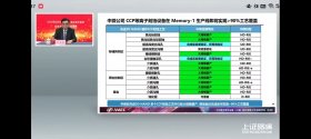
Yes, if you see amec's other presentations. Now it has etching machine for everything.

So once you cover etching for 14nm logic, 19nm dram & 128 layer 3d nand (seems like all 3 will be validated next yr), what's point of buying lam if they can't sell you competitive product?

Btw, if you look at that chart. NAURA & AMEC have full ICP coverage.

They almost have full CCP coverage. But we know from this that AMEC's CCP coverage for NAND is quite good in that most of the items are green (which means they are in mass production already)
AMEC_NAND_CCPCoverage_Sep2023.jpg

So I think this follows what @hvpc and AMEC itself said before. It seems like 3D Nand is further ahead than DRAM.

If I had to guess, expansion with domestic + ASML both restart next year, but Nand maybe a first half kind of thing and DRAM is 2nd half
 
Last edited:

tphuang

Lieutenant General
Staff member
Super Moderator
VIP Professional
Registered Member
If Huawei can offer Nova 5G mid-range smartphones at volume so soon, then our estimation of SMIC capacity might need to revive.
Please, Log in or Register to view URLs content!
well, I posted about this a week ago.

All following Nova phones will be 5G. Nova 12 Pro might use Kirin 9000S and Nova 12 use Kirin 830.

Based on the guy that leaked the Kirin news, they still need some time for the medium range Kirin chips.

So i would probably think wait until December

The interesting part will be whether this new MatePad Pro 13.2 use Kirin (I presume it does). Keep in mind that tablet SoC normally larger and also don't need 5G modem, so you can place more power CPU & GPU in there.


GeekBenchAndroidRankings.png
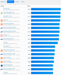
btw, I took. look at Geekbench for multicore scores.

Kirin 9000S on mate 60 pro benchmarked 4206 based on the other photo I posted earlier. That would place it on the same level as Snapdragon 8+ & only beneath Snapdragon 8 Gen 2 & MediaTek 9200 among non Apple SoCs

So, it's peak performance is reasonable for high end chip, of course at expense of greater power consumption
 

huemens

Junior Member
Registered Member

US lawmaker to urge chip industry group to reduce China investments -source​

Please, Log in or Register to view URLs content!

Gallagher planned to tell the group he believes that U.S. rules enacted last October that cut off the sale of advanced artificial intelligence chips to China should be tightened to cover less advanced chips, the source said. The source added that Gallagher also aimed to talk with the group about reducing the number of semiconductor manufacturing machines that could be sent to China.
Also among the planned discussion topics is U.S. investment in Chinese chip firms. Intel, Qualcomm (QCOM.O) and other firms have venture capital arms that have invested in Chinese technology companies, the source added.
 

Phead128

Captain
Staff member
Moderator - World Affairs
Some US cope from Gina:

Please, Log in or Register to view URLs content!

The indecision is palpable.

You'd expect under 'national security' premise that any yield >0% on small-scale unprofitable nodes <14nm to auto-trigger increasingly stricter sanctions, as even small-scale production can satisfy most military application imaginable.

But the cope is from a commercial -scale economic angle, which belies the constant moaning about stopping further military modernization. This strategy is incoherent and unmeasurable.
 
Status
Not open for further replies.
Top