Chinese semiconductor industry

Status
Not open for further replies.

european_guy

Junior Member
Registered Member
A-SET write about Japan tools.

Please, Log in or Register to view URLs content!

Among the 23 export control estrictions that Japan will introduce, this is to me the most critical one:

4. Step-and-repeat and step-scan lithography equipment used to process wafers (the wavelength of the light source is above 193 nanometers, and the value obtained by multiplying the wavelength of the light source by 0.25 and dividing by the numerical aperture is 45 or less). (According to the author's calculation, Nikon's ArF liquid immersion exposure equipment is within the scope of this control, and the exposure equipment before dry etching ArF is not within this scope.)

It means Japan will ban immersion DUV. Now, if also ASML is forced to do the same, this will translate in a stop to 28 / 40 / 45nm nodes capacity build up for China. That would be a heavy blow. SMEE will not be ready for at least another 1/2 years with DUV immersion in volumes enough to cover China demand.

Banning Nikon, even in its entirety, is of course not a problem for China, but the point here is that US is clearly using Japan to force ASML to fully ban DUV immersion.

Lithography is China's Achilles heel. China pays the mismanagement and the indulgence on SMEE along many years, along the biggest part of the last decade. It is just since few years that SMEE is working for real on developing a production lithography machine. Until the SSA600 series included, they were mainly financing-grabbing prototypes, with no real target to be used in the field and no real follow up.

Sorry to be quite direct.
 

tonyget

Senior Member
Registered Member
I agree with the conclusion. That is Huawei has been pushed to a position where it has nothing to lose with announcement of progress,whereas SMIC still has hesitance to do so since they still rely on foreign import to a large degree

Please, Log in or Register to view URLs content!

Why are Huawei, SMIC taking different approaches against US curbs?​


China's tech giant Huawei and top semiconductor foundry SMIC apparently adopt different approaches against US chip curbs. The former has just announced its successful development of electronic design automation (EDA) tools for chips above 14nm process, while the latter has quietly removed 14nm process technology from its service list on its website. What messages are these two Chinese tech players sending through their recent actions? And what are their actual calculations?

At a recent annual financial report conference, Huawei's rotating chairman Xu Zhijun said that over the past three years the company has focused on developing homegrown development tools for hardware, software, and chips amid the lingering US restrictions, and has achieved localization of EDA tools for above 14nm chips and will complete comprehensive verifications this year.

This means that despite its IC design arm HiSilicon suffering a major setback from tough US trade curbs, the successful development of EDA tools for 14nm chips can be said to be a secure self-protection strategy against the risk of being completely cut off by the US in the future.

According to Xu, Huawei's 14nm EDA software, jointly developed with a Chinese EDA vendor, will be incorporated into HiSilicon's chip designs and will also be shared with its partners and customers.

Huawei has not confirmed whether it is also cooperating with China's top EDA developer Empyrean Technology, which specializes in both front- and back-end EDA process nodes for 28nm chips, a mature chip segment with massive applications and with the most capacity expansion momentum at Chinese foundry houses.

Judging from the R&D deployments by Huawei and Empyrean, it seems that they do not want 14/28nm chip designs to be dominated by competitors in Europe and the US and are trying hard to materialize China's autonomy at least in the midrange/mature process nodes.

Then what about SMIC? The foundry has been engaged in mass production of 14nm chips since late 2019, yet with only a single-digit revenue contribution ratio for its most advanced process technology. But it has symbolized SMIC's mass commercial production of FinFET process technology, marking an important first step toward advanced processes in China, though it cannot be on a par with TSMC and UMC in terms of yield rates.

With capital support from the China National Integrated Circuit Industry Fund, also known as the "Big Fund," SMIC's FinFET process advancement is not meant to pursue maximum profits, but to prioritize the import-substitution chips supply and then progress to 7/5nm chips.

SMIC has no other choice but to take its development of FinFET process technology underground, given the upcoming new restrictions on shipments of higher-end DUV machines from Dutch and Japanese suppliers later in 2023. The company has been denied access to EUV lithography equipment supplied by ASML since 2019.

At a recent quarterly earnings call conference, SMIC's co-CEO Zhao Haijun spoke frankly about capacity expansion deployments at its four major manufacturing bases in China. He said its Shenzhen plant has entered volume production of high-voltage driver chips, CMOS image sensor chips, and power electronics chips; its new fab in Tianjin, still under construction, will focus on analog chips and power management ICs (PMIC); and new capacity at fabs in Beijing and Shanghai is set for volume production of multiple chip solutions in the second half of 2023.

But Zhao remained tight-lopped about the current production of 14/12nm chips or development status of more advanced 7/5nm processes at its FinFET wafer fab that has been operational since May 2019. At the current stage, the advanced process base near SMIC's headquarters in Shanghai has become a taboo subject.

The removal of 14nm fabrication technology from SMIC's list of services on its website can be interpreted as a kind of practice designed to give face to the US government in line with its curbs. But it is highly probable that SMIC is eyeing the horizon for future development possibilities.
 
Last edited:

tonyget

Senior Member
Registered Member
havok:嗯,随便举个例子 浸没光刻胶,硅片等等28纳米以下材料的国产化还缺
havok:还有fab运作需要的一系列软件系统的国产化

havok:Well, just to give you an example, the localization of immersion photoresists, silicon wafers and other materials below 28 nanometers is still lacking.
havok:There is also the localization of a series of software systems required for fab operation
 

luminary

Senior Member
Registered Member
Taiwan can be replaced, China CANNOT be replaced, Jensen Huang says.
Please, Log in or Register to view URLs content!

Taiwanese American CEO of NVIDIA denounces US chip sanctions.

“If we are deprived of the Chinese market, we don’t have a contingency for that. There is no other China, there is only one China,” Huang said, adding that there would be “enormous damage to American companies” if they were unable to trade with Beijing.

“If the American tech industry requires one-third less capacity [due to the loss of the Chinese market], no one is going to need American fabs."

“We can theoretically build chips outside of Taiwan, it’s possible [but] the China market cannot be replaced. That’s impossible,” Huang said.
 

gelgoog

Brigadier
Registered Member
Please look at the specs. It's upgraded from 256 TFLOPS to 320 TFLOPS. It's even more powerful than the vaunted A100. And there will be an Ascend 920 coming. Make your own conclusion on what this means, but I think it's pretty obvious.

Ascend-910 is a legit great GPU if it isn't obvious by now. It's competitive by itself in a Atlas-900 PoD vs H100 POD. What does that tell you? Huawei is building a new data center of 16 EFLOPS. These are all things we can prove from video slides. I've watched those videos explicitly and took screenshots.
That does not tell much. With better binning they can overclock the chips they already have so they attain higher performance.
We still have no credible evidence that HiSilicon has an alternative supply for these chips.

"You also have to think about this from a strategic level," the author said. "There's no way China would have blocked any chips from Micron if it would cause extreme damage to the Chinese economy. Obviously, they have probably set up supply chains in place and have chips made in China that are maybe not equal in quality to Micron, but close enough so that they could handle the impact of no more Micron chips coming to China."
Well, that is not 100% correct. While YMTC's product can replace whatever NAND that Micron produces, Micron does also produce DDR5, LPDDR5, GDDR6 DRAM and there is no one in China who can do that yet. CXMT is still stuck with DDR4 and LPDDR4. The thing is, the Chinese government has put in place for several years now rules in place where the machines the government purchases need to have increasing amounts of Chinese made content. But the thing is Samsung and SK Hynix have most of their fab capacity in China. So there is little chance that China will be out of such chips to begin with. Especially when you consider the memory market is in a major slump right now and everyone has been cutting capacity. So right now is an appropriate time to strike.

Taiwan can be replaced, China CANNOT be replaced, Jensen Huang says. "There is only One China."
...
“If the American tech industry requires one-third less capacity [due to the loss of the Chinese market], no one is going to need American fabs."
Exactly. China's market is so huge, it has enough mass to replace all these US products.
 

tphuang

Lieutenant General
Staff member
Super Moderator
VIP Professional
Registered Member
Among the 23 export control estrictions that Japan will introduce, this is to me the most critical one:

4. Step-and-repeat and step-scan lithography equipment used to process wafers (the wavelength of the light source is above 193 nanometers, and the value obtained by multiplying the wavelength of the light source by 0.25 and dividing by the numerical aperture is 45 or less). (According to the author's calculation, Nikon's ArF liquid immersion exposure equipment is within the scope of this control, and the exposure equipment before dry etching ArF is not within this scope.)

It means Japan will ban immersion DUV. Now, if also ASML is forced to do the same, this will translate in a stop to 28 / 40 / 45nm nodes capacity build up for China. That would be a heavy blow. SMEE will not be ready for at least another 1/2 years with DUV immersion in volumes enough to cover China demand.

Banning Nikon, even in its entirety, is of course not a problem for China, but the point here is that US is clearly using Japan to force ASML to fully ban DUV immersion.

Lithography is China's Achilles heel. China pays the mismanagement and the indulgence on SMEE along many years, along the biggest part of the last decade. It is just since few years that SMEE is working for real on developing a production lithography machine. Until the SSA600 series included, they were mainly financing-grabbing prototypes, with no real target to be used in the field and no real follow up.

Sorry to be quite direct.
Again, what's introduced is not all that important, but how it gets implemented is important. Things like whether this is an immediate cease or just not issuing licenses for new orders. That actually makes a big difference. Because as of now, China's sub 45nm capacity is not all that high. The only one really affected will be SMIC and the memory chipmakers. Then the question for them is whether they have enough stocked up and what the implementation looks like.

There is a reason that China is having all these meetings with the Dutch at the moment. I think they've given up on persuading the Japanese and will just retaliate. But wrt Dutch, I think the goal is to buy more time until domestic system is completely ready to fill in.

i do think it's quite obvious that there will be further restrictions from American side on all immersive equipment. Any fabs in China that got comforted by the idea that things will not turn out that way will be very disappointed.

I agree with the conclusion. That is Huawei has been pushed to a position where it has nothing to lose with announcement of progress,whereas SMIC still has hesitance to do so since they still rely on foreign import to a large degree

Please, Log in or Register to view URLs content!

Why are Huawei, SMIC taking different approaches against US curbs?​


China's tech giant Huawei and top semiconductor foundry SMIC apparently adopt different approaches against US chip curbs. The former has just announced its successful development of electronic design automation (EDA) tools for chips above 14nm process, while the latter has quietly removed 14nm process technology from its service list on its website. What messages are these two Chinese tech players sending through their recent actions? And what are their actual calculations?

At a recent annual financial report conference, Huawei's rotating chairman Xu Zhijun said that over the past three years the company has focused on developing homegrown development tools for hardware, software, and chips amid the lingering US restrictions, and has achieved localization of EDA tools for above 14nm chips and will complete comprehensive verifications this year.

This means that despite its IC design arm HiSilicon suffering a major setback from tough US trade curbs, the successful development of EDA tools for 14nm chips can be said to be a secure self-protection strategy against the risk of being completely cut off by the US in the future.

According to Xu, Huawei's 14nm EDA software, jointly developed with a Chinese EDA vendor, will be incorporated into HiSilicon's chip designs and will also be shared with its partners and customers.

Huawei has not confirmed whether it is also cooperating with China's top EDA developer Empyrean Technology, which specializes in both front- and back-end EDA process nodes for 28nm chips, a mature chip segment with massive applications and with the most capacity expansion momentum at Chinese foundry houses.

Judging from the R&D deployments by Huawei and Empyrean, it seems that they do not want 14/28nm chip designs to be dominated by competitors in Europe and the US and are trying hard to materialize China's autonomy at least in the midrange/mature process nodes.

Then what about SMIC? The foundry has been engaged in mass production of 14nm chips since late 2019, yet with only a single-digit revenue contribution ratio for its most advanced process technology. But it has symbolized SMIC's mass commercial production of FinFET process technology, marking an important first step toward advanced processes in China, though it cannot be on a par with TSMC and UMC in terms of yield rates.

With capital support from the China National Integrated Circuit Industry Fund, also known as the "Big Fund," SMIC's FinFET process advancement is not meant to pursue maximum profits, but to prioritize the import-substitution chips supply and then progress to 7/5nm chips.

SMIC has no other choice but to take its development of FinFET process technology underground, given the upcoming new restrictions on shipments of higher-end DUV machines from Dutch and Japanese suppliers later in 2023. The company has been denied access to EUV lithography equipment supplied by ASML since 2019.

At a recent quarterly earnings call conference, SMIC's co-CEO Zhao Haijun spoke frankly about capacity expansion deployments at its four major manufacturing bases in China. He said its Shenzhen plant has entered volume production of high-voltage driver chips, CMOS image sensor chips, and power electronics chips; its new fab in Tianjin, still under construction, will focus on analog chips and power management ICs (PMIC); and new capacity at fabs in Beijing and Shanghai is set for volume production of multiple chip solutions in the second half of 2023.

But Zhao remained tight-lopped about the current production of 14/12nm chips or development status of more advanced 7/5nm processes at its FinFET wafer fab that has been operational since May 2019. At the current stage, the advanced process base near SMIC's headquarters in Shanghai has become a taboo subject.

The removal of 14nm fabrication technology from SMIC's list of services on its website can be interpreted as a kind of practice designed to give face to the US government in line with its curbs. But it is highly probable that SMIC is eyeing the horizon for future development possibilities.
well, it has to stay that way. We just saw Huawei come out with a new V811 chip that likely requires FinFet process. Who could possibly produce that chip or any of the other chips that Huawei got to replace foreign parts? We will continue to have this uncomfortable situation for a while where Huawei introduce new chips that require Finfet process that just magically get produced somewhere.
 

tokenanalyst

Brigadier
Registered Member

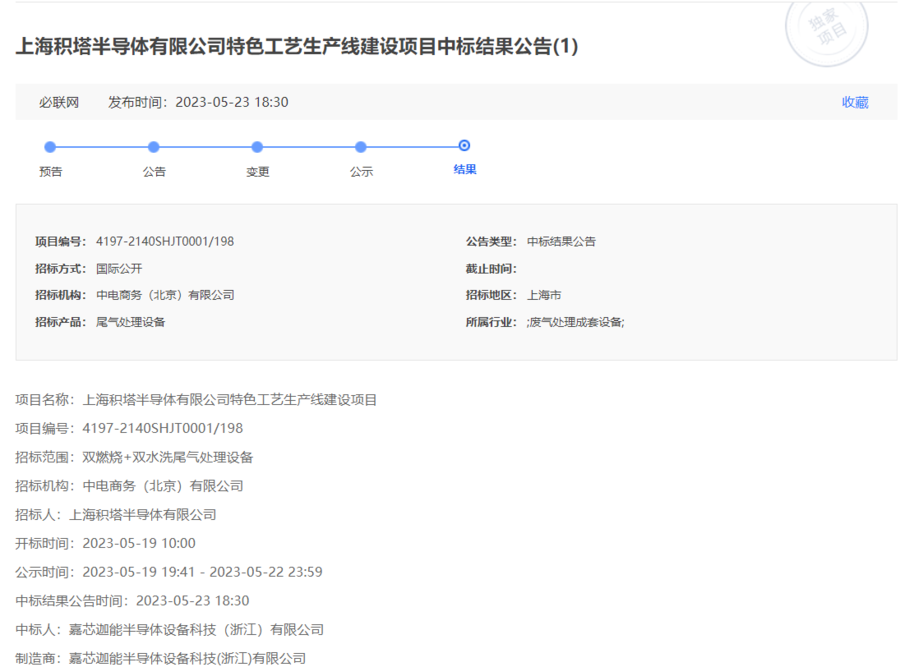
Jiaxin Semiconductor Exhaust Gas Treatment Equipment, a subsidiary of Wanye Enterprise, won the bid for the construction project of a special process production line​


According to the bidding result announcement released by Benetwork on May 23, Wanye Enterprise (600641)'s Jiaxin Cannon's dual-combustion + double-washing exhaust gas treatment equipment won the bid for the construction project of the characteristic process production line, and the number of successful bids was 23 units.

1070954979196.2263.png


It is reported that since the second half of 2022, Jiaxin Semiconductor, a subsidiary of Wanye Enterprise, has won multiple bids for various equipment. Including silicon nitride plasma etching machine, metal plasma etching machine, side wall plasma etching machine, high density plasma film deposition equipment (HDP-CVD), silicon dioxide plasma film deposition equipment (PECVD), doped boron phosphorus Silicon oxide thin film chemical deposition equipment (SACVD), titanium/titanium nitride deposition equipment (MOCVD), aluminum copper metal sputtering equipment (PVD) and rapid thermal processing (RTP), etc.

Wanye Enterprise continues to support the growth and research and development of domestic equipment, and deploys the semiconductor equipment and material track with a two-wheel drive strategy of independent research and development and epitaxial mergers and acquisitions. At present, the company's Kaishitong and Jiaxin Semiconductor have superimposed to form multiple semiconductor front-end core equipment product lines, and their business covers ion implanters, etching machines, thin film deposition, rapid heat treatment and other types of equipment. With the unique domestic "1+N" semiconductor equipment platform company's multi-category track, the company is committed to promoting the butterfly change and leap of China's integrated circuit industry.

Please, Log in or Register to view URLs content!
 

tokenanalyst

Brigadier
Registered Member
Among the 23 export control estrictions that Japan will introduce, this is to me the most critical one:

4. Step-and-repeat and step-scan lithography equipment used to process wafers (the wavelength of the light source is above 193 nanometers, and the value obtained by multiplying the wavelength of the light source by 0.25 and dividing by the numerical aperture is 45 or less). (According to the author's calculation, Nikon's ArF liquid immersion exposure equipment is within the scope of this control, and the exposure equipment before dry etching ArF is not within this scope.)

It means Japan will ban immersion DUV. Now, if also ASML is forced to do the same, this will translate in a stop to 28 / 40 / 45nm nodes capacity build up for China. That would be a heavy blow. SMEE will not be ready for at least another 1/2 years with DUV immersion in volumes enough to cover China demand.

Banning Nikon, even in its entirety, is of course not a problem for China, but the point here is that US is clearly using Japan to force ASML to fully ban DUV immersion.

Lithography is China's Achilles heel. China pays the mismanagement and the indulgence on SMEE along many years, along the biggest part of the last decade. It is just since few years that SMEE is working for real on developing a production lithography machine. Until the SSA600 series included, they were mainly financing-grabbing prototypes, with no real target to be used in the field and no real follow up.

Sorry to be quite direct.
Is export controlled not necessary means banned. The problem with Nikon is that they only produce only two types of immersion scanners "NSR-S635E and NSR-S625E" that TRY to compete with the ASML scanners that the Netherlands put in their control list, Nikon doesn't have the capacity to maintain legacy scanners the same way ASML does, they produce NXT:2100, NXT:2050 and the legacy ones NXT:2000, NXT:1980, NXT1970.

The Japanese goverment is so cucked that they literally make things difficult for Nikon and gain nothing from it.

Please, Log in or Register to view URLs content!

I still think that China should treat lithography as critical even against the will of fab managers and even if that means straining a little the relationship with ASML and the Netherlands. They need put an aggressive war-like effort developing these systems and building manufacturing capacity for these systems. If it wasn't for lithography systems I would dare to say that China could make it own their own even without the input of the Japanese.
 

tokenanalyst

Brigadier
Registered Member

Wuhu's third-generation semiconductor industry enters the "fast lane"​


A few days ago, the reporter learned from the strategy conference held by Anhui Changfei Advanced Semiconductor Co., Ltd. that, as one of the leading enterprises in the third-generation semiconductor industry in our city, its Wuhu base has an annual production capacity of 60,000 SiC MOSFET wafers. It provides strong support for our city to build a national third-generation semiconductor industry highland.
Since last year, the company has successfully completed mergers, reorganizations, and integrations. It has formed a full industrial chain capability from design, epitaxy, wafer manufacturing to module packaging and testing from the past foundry development, and has established systematic product development, product management, and business Expanding capabilities, creating a complete 650V-3300V SiC product matrix, achieving full coverage from photovoltaics, energy storage, charging piles to new energy vehicles and other application fields, and further improving the professional SiC wafer foundry service system. On the basis of the Wuhu base gaining momentum, the company will also start the construction of the Wuhan base project with an annual output of 360,000 SiC MOSFETs, including epitaxy, device design, wafer manufacturing, packaging, etc., and its production capacity ranks in the leading position in the industry. The rapid development momentum of the company has also attracted the attention of the capital market. The A round of equity financing is progressing smoothly, and is expected to set a record for a single private equity financing since the development of the third-generation semiconductor in China.


Please, Log in or Register to view URLs content!
 

tokenanalyst

Brigadier
Registered Member

SDIC Entrepreneurship leads the investment in Huaxun Semiconductor, an advanced packaging material company​


Huaxun Semiconductor was established in 2016 by the technology transfer and transformation of Shenzhen Institute of Advanced Technology, Chinese Academy of Sciences. It is a national high-tech enterprise focusing on the research and development and sales of advanced electronic materials. The company focuses on the fields of advanced packaging of integrated circuits, compound semiconductors, and new displays, and provides customers with system solutions and key materials. The company and Shenzhen Advanced Electronic Materials International Innovation Institute jointly established a joint laboratory to realize scientific research transformation, pilot test and customer verification, filling the domestic gap.

The technical threshold of high-end electronic materials is high, and the current domestic market is mainly monopolized by American and Japanese companies. The ultraviolet laser debonding material independently developed by Huaxun Semiconductor has successfully achieved large-scale application, helping the mass production of advanced packaging of domestic high-end server chips. This technology won the second prize of Shenzhen Science and Technology Progress Award. Thermal slip temporary bonding materials mainly serve leading domestic compound semiconductor customers such as CETC and Sanan Optoelectronics.

For the Cu-Low K process of compound semiconductors and integrated circuits, Huaxun Semiconductor has successfully developed a series of water-soluble protective liquid products for its laser cutting process, which can greatly protect the surface of the wafer and inhibit the adhesion of debris. Thermal fixation of the protective film. In the field of new displays, based on the underlying innovation of polymer material design and synthesis, Huaxun Semiconductor has successfully developed laser release materials and high-yield materials that can meet the mass transfer of Micro LEDs, supporting the pilot mass production of leading domestic display companies.​

In the future, Huaxun Semiconductor will keep up with market demand, increase investment in innovative research and development, and continue to tackle high-end electronic materials that are urgently needed in my country. solutions to empower the development of the pan-semiconductor industry.

1684948053654.png

Please, Log in or Register to view URLs content!
 
Status
Not open for further replies.
Top