My article on TSMC from Seeking Alpha has been translated and published, showing the strength of Taiwan fabs. The link is here:Is south korea's current restriction by the America overall good or bad for China? On one hand, decreased levels of investment and restricted sales to China from SK will hurt China in the short term, who can still benefit from SK's knowledge and equipment. And it will reduce SK's dependence on China and increase SK's dependence on America, making them even more of US lapdog than they were before.
On the other hand, it could make SK realise just how dependent they are on American technology and try to replace it, maybe even with some chinese techolongy. Long term, lacking access to the chinese market also means that SK won't be competitive in the long run. It also gives China an good excuse to retaliate in other ecomnic ways, and when China's equipment and semiconductor techologny catches up, completely run SK out of the market alltogethor with a very reasonable excuse of "How can you be a trusted trading partner if you're willing to knee to America and cut me off buying your equipment, how can I be sure that you won't do the same for other products?"
What does SK still make that China can't come up with a domestic substitute anyway? They do seem very much less important in the equipment/photoresist space than Japan. And their Fabs still can't complete with Taiwan.

You are using an out of date browser. It may not display this or other websites correctly.
You should upgrade or use an alternative browser.
You should upgrade or use an alternative browser.
Chinese semiconductor industry
- Thread starter Hendrik_2000
- Start date
- Status
- Not open for further replies.
Full EUV power on laboratory scale: Researcher awarded for the development of compact high-power EUV source
The future has a color: it is extreme ultraviolet. With the help of EUV light it is possible, for example, to produce smaller and more powerful microchips than ever before. But further research faces a problem: Experiments with laser-like EUV light can usually only be conducted at expensive large-scale research facilities. Jena scientist Robert Klas wants to change that. He has developed a compact EUV laser module that can be used to generate this special light much more cost-effectively. Potential applications are possible in semiconductor manufacturing and microscopy. Robert Klas has now been awarded the Hugo Geiger Award for his work.
Researcher Robert Klas from Jena has developed a compact module for generating laser-like EUV light as part of his doctoral thesis. Where research facilities the size of an entire house have been necessary so far, so-called synchrotrons, Klas now presents a new and efficient method to generate laser-like EUV light in a facility the size of a laboratory bench.
Klas' doctoral thesis, which is the result of cooperation between the Friedrich Schiller University Jena, the Helmholtz Institute Jena and the Fraunhofer Institute for Applied Optics and Precision Engineering IOF, provides the most powerful laser-like EUV source on a laboratory scale to date, with an average power of 10 milliwatts - a hundred times more power than the state-of-the-art in comparable systems when he began his doctorate. This will make EUV research more independent of large-scale facilities that are costly to maintain. In addition, the compact setup costs only a fraction.
EUV source on laboratory scale with one hundred times more power
In his work, Klas is addressing a major challenge in laser optics. An important principle here is that the shorter the wavelength, the harder it is to generate laser radiation. In his research, the physicist is working in the wavelength range from 10 to 50 nanometers. One nanometer corresponds to one millionth of a millimeter. In short, extreme ultraviolet light is extremely difficult to generate directly as laser light.
To solve this problem, Klas uses modern high-power ultrashort pulse fiber lasers. These are converted into EUV light using the process of high harmonic generation. To do this, Klas first focuses the high-power laser in an inert gas. In this process, electrons are accelerated within a few 100 attoseconds. An attosecond is one quintillion of a second. Robert Klas illustrates this order of magnitude with a comparison: »An attosecond is to a second what a second is to our world age,« he explains. The electrons accelerated in this unimaginably short time subsequently produce the precious EUV radiation by recombining with their parent ion.
The main challenge is to coherently superimpose the released radiation, i.e., to control it in such a way that its so-called wave crests in the extreme ultraviolet spectrum add up and can be bundled into a laser beam at the end. Through the correct choice of laser parameters as well as gas density, he has succeeded in generating EUV radiation with laser-like parameters in a highly efficient manner. In combination with high-power driver lasers, this has led to a significant increase in EUV performance.
High-power EUV source sets a new standard in high-resolution microscopy
The scientist is convinced that his work will significantly facilitate further research and application of EUV light: »In the future, the results of my doctoral thesis are expected to drive development in many key areas such as the energy and storage efficiency of chips as well as biology and medicine.«
During his research, Klas already tested the first potential applications for his novel EUV source on a laboratory scale. In exchange with other researchers, he has turned his attention to lens-less microscopy in particular - specifically imaging in the range of tiny nanometers. »With an exposure wavelength of 13.5 nanometers, we have realized a resolution of 18 nanometers, « he reports. By comparison, conventional light microscopes only manage a resolution of just under 500 nanometers. Klas uses another example to illustrate the incredible detail of the microscopy made possible by EUV light: »In one experiment, we achieved a so-called field of view measuring 100 x 100 micrometers. That means we can comparatively cover the size of a soccer field within an image and find a coin in it.«
A further innovation: with EUV-based microscopy, colored images of a sample under investigation can be generated. In this way, researchers can »look inside a cell« and distinguish different elements or proportions of different substances such as carbon, lipids, etc. - »a novelty at such a high resolution,« Klas emphasizes. »With our technology, we can use this to advance biological and medical studies in the future and hopefully study different types of viruses. At some point, we also want to be able to image DNA with a diameter of about two nanometers using this method,« says the scientist.
Quality assurance in semiconductor manufacturing using EUV lithography
Another special application potential is offered by the technology developed by Klas in the field of EUV lithography. Here, tiny microchips are manufactured using extreme ultraviolet light. The semiconductor industry already uses this process to apply more than ten billion transistors to a chip the size of a fingernail. A research team from TRUMPF, ZEISS and Fraunhofer was awarded the German Future Award in 2020 for the development of EUV lithography.
Klas' research opens a new possibility for quality assurance in this context. This is because the outstanding microscopic properties of his system can also be applied to an exposure mask. This is used in semiconductor manufacturing to produce the tiny EUV chips. If there are defects in this mask, they are passed on to the chips manufactured with it. EUV microscopy can be used to examine the mask for such defects. Detecting weak spots in the EUV mask early on and thus avoiding further errors in production saves time and money. »This process can reduce waste and thus lead to more sustainable production,« says Klas, explaining the benefits of this method.
Honored with the Hugo Geiger Award
Robert Klas has now been awarded the »Hugo Geiger Award for Young Scientists« for his groundbreaking work. The award is granted by the Free State of Bavaria and the Fraunhofer-Gesellschaft to outstanding young researchers. The award ceremony took place on March 21 in Munich. A total of three scientists from Munich, Freiburg and Jena were honored. For further information on the award and the other award winners, please see the press release of the Fraunhofer-Gesellschaft:
EUV light - the light for the digital age
Light in the extreme ultraviolet range, or EUV light for short, is a very special light. Due to its particularly short wavelength, it can be used to produce tiny structures. This is important in semiconductor manufacturing, for example: Here, EUV light can be used to produce ultra-fine circuits on microchips. This way, semiconductors can be made smaller and at the same time more powerful than ever before. And it is these mini-chips that we urgently need, because without them, progress in artificial intelligence and autonomous driving, for example, would be virtually inconceivable.
Until now, the generation of laser-like EUV light has only been possible in expensive and complex large-scale facilities. Researchers must visit special research centers, so-called synchrotrons, to use these facilities. Scientists often wait years for a place here, to experiment only for a few weeks or even days. Research and further technological progress, which EUV light promises especially in the digital age, are thus massively impeded. Klas aims to remedy this situation in the future with the new, compact EUV source.
this is kind of interesting. Bloomberg is saying now that the CHIPS act is not turning out to what it should be. It does make me wonder that given the anti-business stuff that Biden administration is putting into CHIP act implementation, if that will cause more firms to reconsider their participation in it. I'm not saying it's a loss for China to not be getting more Korean/Taiwanese fab expansions, but reduced expansion by Samsung and SK will have affect on YMTC and CXMT. Similarly, one could argue that TSMC expanding 28nm capacity in China is a good or a bad thing.
@hvpc would know the best here, but from what i can tell, CXMT is having enough trouble with the October sanctions that it is sticking with 19/21nm DRAM production for the near term.Does anyone know whether any chinese companies are working on making GDDR5/6/7 memory chips?
Indeed, no one domestically is currently capable of building chips for DDR5 or GDDR5. If I recall, DDR5 are made with minimum of D1z node or ~16-17nm node. CXMT is HVM on their second generation (D1x or 19nm node) was still working to rollout 18nm node or D1y when the tighter US sanction hit last October. So not close to able to support DDR5/GDDR5 yet.@hvpc would know the best here, but from what i can tell, CXMT is having enough trouble with the October sanctions that it is sticking with 19/21nm DRAM production for the near term.
this doesn’t mean no one is working to circumvent the 18nm limit imposed by the US. CXMT, YMTC, CHJS, and Swaysure are all exploring ways (3D DRAM, IGZO 1T0C DRAM, other 4F2 DRAM methods) to circumvent the YUS sanction to achieve DRAM with bit density equivalent to D1z and below. Everyone’s technical roadmap timing are mostly set fir 2024/25. So we will see if one of these guys could come up with something that could support DDR5/GDDR5.
As for the DRAM market in general, Samsung had indicated they target to rollout DDR6 in 2025. We will worry about DDR6 after we can conquer DDR5 first.


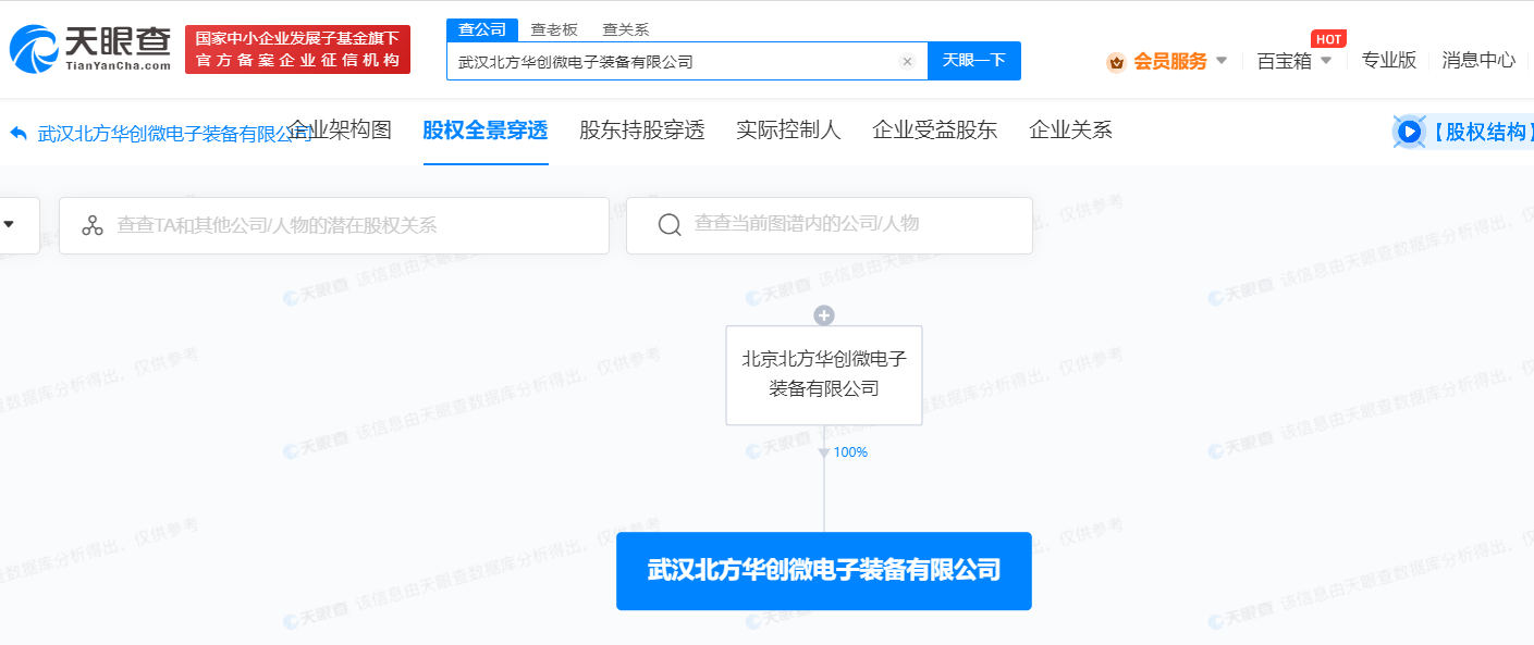
North Huachuang established a microelectronic equipment company in Wuhan with a registered capital of 25 million yuan
According to Weibo news, Tianyan Check shows that recently, Wuhan North Huachuang Microelectronics Equipment Co., Ltd. was established, the legal representative is Liu Lijian, the registered capital is 25 million yuan, and the business scope includes the manufacture of electronic special equipment; sales of electronic special equipment; special equipment repair; Mechanical parts, spare parts processing; sales agents, etc.
Source: Tianyancha
The equity penetration chart shows that the company is wholly owned by Beijing North Huachuang Microelectronics Equipment Co., Ltd.
It is reported that North Huachuang is an advanced enterprise of high-end integrated circuit technology equipment in China. Its main products include high-end semiconductor technology equipment and core components such as etching machines, PVD, ALD, CVD, oxidation/diffusion furnaces, cleaning machines, and gas mass flow meters. , are widely used in integrated circuits, advanced packaging, semiconductor lighting, micro-electromechanical systems, power semiconductors, compound semiconductors, new energy photovoltaics, flat panel displays and other fields, providing solutions for semiconductors, new energy, new materials and other fields.
It is reported that North Huachuang is an advanced enterprise of high-end integrated circuit technology equipment in China. Its main products include high-end semiconductor technology equipment and core components such as etching machines, PVD, ALD, CVD, oxidation/diffusion furnaces, cleaning machines, and gas mass flow meters. , are widely used in integrated circuits, advanced packaging, semiconductor lighting, micro-electromechanical systems, power semiconductors, compound semiconductors, new energy photovoltaics, flat panel displays and other fields, providing solutions for semiconductors, new energy, new materials and other fields.
Tongfu Microelectronics: In 2022, the operating income will be 21.428 billion yuan, a year-on-year increase of 35.52%.
According to news from Jiwei.com, on the evening of March 29, Tongfu Microelectronics Co., Ltd. (hereinafter referred to as "Tongfu Microelectronics") released its 2022 annual report. During the reporting period, it achieved operating income of 21.429 billion yuan, a year-on-year increase of 35.52%; The net profit attributable to shareholders of the parent company was 502 million yuan, a year-on-year decrease of 47.53%; the net profit attributable to shareholders of the parent company should be 713 million yuan, a year-on-year decrease of 25.46%.
According to the newspaper, affected by exchange rate fluctuations, Tongfu Microelectronics incurred exchange losses, thus reducing the net profit attributable to shareholders of the parent company by 211 million yuan. In addition, due to the declining prosperity of the integrated circuit industry and weak demand for some end products, Tongfu Microelectronics’ capacity utilization rate and gross profit margin have declined; Tongfu Microelectronics has increased R&D investment in advanced packaging technology innovation such as Chiplets, and R&D expenses have increased, leading to a decrease in profits. decline.
During the reporting period, Tongfu Microelectronics has achieved fruitful technological innovation results: the self-built 2.5D/3D production line is fully connected, the research and development of 1+4 products and 4-layer/8-layer stacked products is steadily advancing; the Fan based on the Chip Last process -out technology, realize 5-layer RDL ultra-large size package (65×65mm); super multi-chip FCBGA MCM technology, realize up to 13 chip integration and super-large package above 100×100mm.
- Status
- Not open for further replies.