You are using an out of date browser. It may not display this or other websites correctly.
You should upgrade or use an alternative browser.
You should upgrade or use an alternative browser.
Chinese semiconductor industry
- Thread starter Hendrik_2000
- Start date
- Status
- Not open for further replies.
We assume that he knows a lot or has deep expertise just because he's willing to talk. It could be that he doesn't know as much as we think.It's also amusing to me that he went from grating interferometer not ready and may not be doable to planar gratings is almost there in like a month. What changed?
We assume that he knows a lot or has deep expertise just because he's willing to talk. It could be that he doesn't know as much as we think.
The way he talks, he sounds like the boss.
And the boss, never tells everything.
They only hint, and the hints tend to come true.
He knows that, because he's the boss.
a professional manufacturing enterprise in the instrumentation industry, Changchun Yuheng Optics Co., Ltd. has been focusing on the research and development of grating sensors, and has now developed into a leading enterprise in the subdivided industry. The annual production capacity of the leading product grating encoders reaches 1.5 million units
I'm actually curious how much of this is happening. We hear that de-americanized production lines for SMIC Beijing plant will be at 28nm this year. We also see that they've had issue with expanding their capacity at SMSC plants, because American tools have been restricted for a while. We also know that China's own tools industry cannot fully supply 14nm or lower production, so many tools need to be imported (and it's more than just lithography machine). It's unclear if SMIC has been able to expand capacity with alternatively sourced American tools or with tools from other countries.
SMIC's full year report will be interesting.
SMIC's full year report will be interesting.
I do enjoy reading some of Dylan Patel's freakout sometimes like this one
Yes, by being slaves to paying dividends, Intel is making moves that will lead to serious Talent draining.
interesting look here on Moores law
single thread performance has basically already peaked and CPU designers are just packing int more cores now.
Yes, by being slaves to paying dividends, Intel is making moves that will lead to serious Talent draining.
interesting look here on Moores law
single thread performance has basically already peaked and CPU designers are just packing int more cores now.
We are just getting to the point of more advanced packaging. It's good news for China since once they can comfortably produce 5 to 7 nm chips, then packaging will matter a lot more than just how many transistors you can pack in there.• Stage I, when transistor density is governed by Dennard Scaling, extends from formulation in 1965 to roughly 2005 (“Moore’s Bend”).
• Stage II results as semiconductor dies are expanded in size horizontally (“bigger chips”), usually by increasing core counts (a core is a small CPU or processor built into larger CPU). Stage II extends from around 2005 to 2020 when die sizes reach a practical limit.
• Stage III begins when semiconductor dies are first scaled vertically, and then extends later with new steps to keep Moore’s Law alive: complex 3D structures, and more materials, architectures, connectivity options, and packaging advances (chiplets, etc.). The impact will be astonishing: all industry will have to change from design through manufacturing to process control and testing to realize the changes in Stage III.
Is difficult to know because usually this sites never publish their sources as always, I take what this guy is saying with a truck load of salt. But they could be buying used tools for spare parts because US companies cannot service their fabs. Until they design out US tools from their processes.I'm actually curious how much of this is happening. We hear that de-americanized production lines for SMIC Beijing plant will be at 28nm this year. We also see that they've had issue with expanding their capacity at SMSC plants, because American tools have been restricted for a while. We also know that China's own tools industry cannot fully supply 14nm or lower production, so many tools need to be imported (and it's more than just lithography machine). It's unclear if SMIC has been able to expand capacity with alternatively sourced American tools or with tools from other countries.
SMIC's full year report will be interesting.
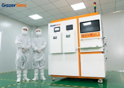
GEZE Technology's first FTIR wafer measurement equipment was successfully delivered, helping the localization of semiconductor equipment!
GEZE Technology's first FTIR wafer measurement equipment GS-M08X was successfully delivered to a well-known domestic semiconductor manufacturer. The semiconductor testing equipment delivered this time is independently developed and produced by GEZE Technology, and the equipment will be used in the front-end measurement of semiconductors.Fourier transform infrared wafer measurement equipment is an indispensable key equipment in the wafer inspection process. The optical system of this equipment is highly complex and has been highly monopolized by foreign manufacturers such as Onto innovation, Thermo Scientific, and Semilab for a long time, and the domestic market is heavily dependent on imports. Taking advantage of its senior research experience in the field of optics, GEZE Technology has continuously explored and opened up new directions, concentrated its efforts on precision optical technology, and independently developed the first FTIR Fourier transform infrared wafer measurement equipment.

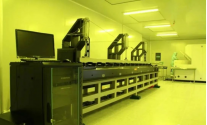
The GS-M08X inspection equipment delivered this time consists of a custom-developed optical system, an automated wafer inspection machine, and semiconductor professional analysis software . Imported Robot and Aligner ; and Load Port and control software independently designed and developed by GEZE Technology are adopted . The equipment occupies a small area, adopts a multi-axis manipulator, and realizes picking and unloading and detection positioning through compound precision motion, which greatly improves the detection efficiency and reduces product maintenance costs. The newly designed gas guide structure inside ensures the cleanliness of the wafer transfer process. Multiple interlock protections, from software to hardware, ensure the safety of the wafer transfer process and the safety of personnel and equipment. Combined with its advanced and efficient analysis software, it provides the best solution for semiconductor wafer front-end measurement.
Recently, the Yangtze River Delta National Technology Innovation Center and Baoshan District held the "Yangtze River Delta National Innovation Center-Baoshan District Cooperation Project Signing Conference". At the meeting, Baoshan High-tech Zone signed a contract on the laser crystal material project.
The laser crystal material project, led by Dr. Dong Yongjun from the Shanghai Institute of Optics and Mechanics, Chinese Academy of Sciences, focuses on the independent research and development of the core technology and process of crystal material bonding, realizes glue-free bonding of laser functional materials, heat dissipation materials and other materials, and greatly simplifies laser devices The advanced packaging steps can not only directly improve the heat dissipation performance and reduce the packaging cost, but also effectively improve the reliability and stability of the laser, and promote the miniaturization of laser device packaging technology. At present, the product has passed the test and verification of laboratory-level bonding equipment, and has provided samples for the application side. The "eye-safe laser bonding crystal and device" developed by the team provides solutions for integrated laser materials and miniaturized laser devices in the eye-safe band, and provides solutions for laser radar applications such as automotive autonomous driving, laser ranging, and laser mapping. Safer and more reliable "eyes".
According to the agreement, the project will expand the commercial application of laser crystal materials and devices in automotive radar, ranging, surveying and mapping, medical treatment, semiconductor processing and other fields, and further expand its independent core technology and device products in automotive, industrial and civilian consumption High-level and military applications, and create innovation-leading advantages in market segments. The project will also further enrich the new material industry ecology of Baoshan High-tech Zone, focus on the park's adherence to the integration of "scientific innovation + industry", focus on key technical fields and key links, help my country's cutting-edge technology, and enhance international competitiveness.
- Status
- Not open for further replies.

