Chinese semiconductor industry

Status
Not open for further replies.

tokenanalyst

Brigadier
Registered Member

Guanglinda : Fully automatic ultrasonic scanning equipment helps the development of IGBT/SiC industry​

As semiconductor devices have higher and higher requirements on the manufacturing process. Since defects such as voids, cracks, and delamination in the solder layer may lead to failure of semiconductor devices in long-term operation, the market urgently needs a non-destructive testing tool with high resolution, high sensitivity, and very sensitive to the bonding surface.

Recently, Suzhou Guanglinda Electronic Technology Co., Ltd. (referred to as "Guanglinda") developed the first fully automatic ultrasonic scanning equipment (GRD-CS3 ) in China and sent it to an international factory. The equipment can automatically complete a complete set of scanning processes . , while ensuring high efficiency, high precision and high intelligence, it saves labor costs, and meets the needs of mass production of customers with high quality. For the first time, it has realized the localization of ultrasonic testing equipment in the field of advanced packaging chips. IGBT/SiC ) defect identification ability has been widely recognized by customers.

1664210758862.png


Please, Log in or Register to view URLs content!
 

weig2000

Captain
A Stratechery newsletter/post on Nvidia: its ambition and audacity, and the associated challenges. The Stratechery is a pretty well-known podcast and newsletter focusing tech landscape and analysis. This one is a bit longish, but worth reading. Some years ago, a Google recruiter reached out to me for a potential opportunity in the company. He gave me a list of readings to prepare for the upcoming interviews; Stratechery is one of them. Interestingly, the author is an American but is based out of Taiwan.

Please, Log in or Register to view URLs content!

Some interesting excerpts:

Here’s the problem, though: all of that dedicated hardware comes at a cost. Nvidia’s new GPUs are big chips — the top-of-the-line AD102, sold as the RTX 4090, is a fully integrated system-on-a-chip that measures 608.4mm2 on TSMCs N4 process; the top-of-the-line Navi 31 chip
Please, Log in or Register to view URLs content!
, in comparison, is a chiplet design with a 308mm2 graphics chip on TSMC’s N5 process, plus six 37.5mm2 memory chips on TSMC’s N6 process. In short, Nvidia’s chip is much larger (which means much more expensive), and it’s on a slightly more modern process (which likely costs more).

Nvidia's chips are very high-end and expensive. They need to create a vision and future for people to justify the high price and high margin of their chips.

In Huang’s view, simply having fast chips is no longer enough for the workloads of the future: that is why Nvidia is building out entire data centers using all of its own equipment. Here again, though, a future where every company needs accelerated computing generally, and Nvidia to build it for them specifically — Nvidia’s Celestial City — is in contrast to the present where the biggest users of Nvidia chips in the data center are hyperscalers who have their own systems already in place.

A company like Meta, for example, doesn’t need Nvidia’s networking; they
Please, Log in or Register to view URLs content!
. What they do need are a lot of massively parallelizable chips to train their machine learning algorithms on, which means they have to pay Nvidia and their high margins. Small wonder that Meta, like Google before them, is
Please, Log in or Register to view URLs content!
.

This is the course that all of the biggest companies will likely follow: they don’t need an Nvidia system, they need a chip that works in their system for their needs. That is why Nvidia is so invested in the democratization of AI and accelerated computing: the long term key to scale will be in building systems for everyone but the largest players. The trick to making it through the valley will be in seeing that ecosystem develop before Nvidia’s current big customers stop buying Nvidia’s expensive chips. Huang once saw that 3D accelerators would be commoditized and took a leap with shaders; one gets the sense he has the same fear with chips and is thus leaping into systems.

Same with the data centers and hyperscalers in China, they will need to either develop their own AI chips or work with Chinese chip vendors to lower the cost, above and beyond all the risks and nonsense associated with the US sanctions.
 

tokenanalyst

Brigadier
Registered Member

Growing FPGA market in China.

FPGA localization process accelerates interface IP manufacturers to welcome the highlight moment​


From the micro-net news, in the chip track where hundreds of flowers bloom, FPGAs developed from logic verification have long become an important member of the processor chip family.

FPGA (Field Programmable Gate Array) is a field programmable gate array, which is a semiconductor device that can realize the logic circuit required by the user through reprogramming. Compared with CPU, GPU, and ASIC chips, the underlying algorithm of FPGA chips is not solidified, and has the characteristics of programmability, high performance, low energy consumption and flexibility, and has both hardware parallelism and low latency. And the cost advantage is obvious.

Compared with other tracks, FPGA is a relatively niche market, far less than the market size of tens of billions of dollars in the CPU and GPU fields. However, it plays an irreplaceable role in communications, data centers, industrial applications and other fields, and is an important artificial intelligence-related chip. In recent years, with the rise of AI computing, 5G communication, and heterogeneous computing, the value of FPGA has become more and more prominent.

FPGA localization process is accelerated

Thanks to its high degree of flexibility and powerful parallel processing capabilities, FPGAs can play a role in all applications in the cloud, on the end, and in the middle, and the market size continues to expand. According to the statistics of market research firm Frost & Sullivan, the global market size of FPGA has increased from about 4.34 billion US dollars in 2016 to about 6.08 billion US dollars in 2020, with an average annual compound growth rate of about 8.8%. With the continuous growth of the global demand for new-generation communication equipment and emerging fields such as artificial intelligence and autonomous driving technology, the global FPGA market size is expected to grow from US$6.86 billion in 2021 to US$12.58 billion in 2025, with an average annual compound growth rate of about was 16.4%.

Compared with the global market, the Chinese market is growing more rapidly. According to Frost & Sullivan data, China's FPGA market has grown from about 6.55 billion yuan in 2016 to about 15.03 billion yuan in 2020, with a compound annual growth rate of about 23.1%. With the further acceleration of the domestic substitution process, it is expected that the size of China's FPGA market will reach about 33.22 billion yuan by 2025, with a CAGR of 16.6% in 2020-2025.

Please, Log in or Register to view URLs content!
 

Jianguo

Junior Member
Registered Member
New architecture also works. I'm not an expert in architecture but GAA doesn't necessarily need a dieshrink.

This paper shows 17-20 nm lateral CD, which is within DUV range.

Please, Log in or Register to view URLs content!

Compare to FinFET fin width for 14 nm which has 8-10 nm lateral width requirements.

Please, Log in or Register to view URLs content!

This paper shows 50 nm CD and deposition using Applied Materials Producer 200 and Centaur 200 which came out in the 1990s for 200 mm wafers. Etch was done on a Lam TCP 9400DFM from the 1990s as well.

Please, Log in or Register to view URLs content!
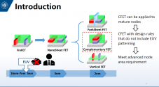
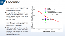
This nVSAFET architecture looks like a variation on the CFET architecture @tokenanalyst posted about not long ago. Both nVSAFET and CFET have vertical stack structures using nanowires/nanosheets. Like wafer bonding but on the architecture level. What I find very interesting is nVSAFET claims design goals similar to GAAFET for 3nm and beyond without stating what you pointed out about its possible application with DUV. CFET actually summarizes what you said in that paper's "Intro" and "Conclusion". Intro and Conclusion clearly state that CFET can be applied with DUV.

1664244294247.png1664244128738.png
I don't know if I'm fully understanding this, but these architectures look like they can achieve equivalent 5nm and 7nm using DUV WITHOUT multi-patterning, as is necessary with FinFET. If so, China's lithography machines wouldn't need overlay precision <2.1nm to create equivalent 5nm/7nm. They could even use their older NXT:1950 machines and still create what would need the NXT:2100 using FinFET. I'm sort of fantasizing right now so maybe somebody can correct me? :oops:
 

ansy1968

Brigadier
Registered Member
This nVSAFET architecture looks like a variation on the CFET architecture @tokenanalyst posted about not long ago. Both nVSAFET and CFET have vertical stack structures using nanowires/nanosheets. Like wafer bonding but on the architecture level. What I find very interesting is nVSAFET claims design goals similar to GAAFET for 3nm and beyond without stating what you pointed out about its possible application with DUV. CFET actually summarizes what you said in that paper's "Intro" and "Conclusion". Intro and Conclusion clearly state that CFET can be applied with DUV.

View attachment 98293View attachment 98292
I don't know if I'm fully understanding this, but these architectures look like they can achieve equivalent 5nm and 7nm using DUV WITHOUT multi-patterning, as is necessary with FinFET. If so, China's lithography machines wouldn't need overlay precision <2.1nm to create equivalent 5nm/7nm. They could even use their older NXT:1950 machines and still create what would need the NXT:2100 using FinFET. I'm sort of fantasizing right now so maybe somebody can correct me? :oops:
Bro you're a good teacher, explaining such technical term for us common layman to understand, I appreciate it so much! :) So from your explanation it's possible, they are researching and improving the DUVL tech with ASML until a viable Chinese EUVL is introduced. Now my question is will these become mainstream and make EUVL redundant?
 

FairAndUnbiased

Brigadier
Registered Member
This nVSAFET architecture looks like a variation on the CFET architecture @tokenanalyst posted about not long ago. Both nVSAFET and CFET have vertical stack structures using nanowires/nanosheets. Like wafer bonding but on the architecture level. What I find very interesting is nVSAFET claims design goals similar to GAAFET for 3nm and beyond without stating what you pointed out about its possible application with DUV. CFET actually summarizes what you said in that paper's "Intro" and "Conclusion". Intro and Conclusion clearly state that CFET can be applied with DUV.

View attachment 98293View attachment 98292
I don't know if I'm fully understanding this, but these architectures look like they can achieve equivalent 5nm and 7nm using DUV WITHOUT multi-patterning, as is necessary with FinFET. If so, China's lithography machines wouldn't need overlay precision <2.1nm to create equivalent 5nm/7nm. They could even use their older NXT:1950 machines and still create what would need the NXT:2100 using FinFET. I'm sort of fantasizing right now so maybe somebody can correct me? :oops:
this is very interesting. So this is my thinking based on that picture, and I might be off the mark wildly here, what they're doing is taking the smallest gate dimension from lateral CD (as in FinFET, which is now at 8-10 nm fin width) to a thickness. While small lateral CD requires high resolution and overlay precision lithography, the CFET and VFET architectures requires precision in film thickness. Since China's deposition and etch control is more advanced than lithography, this plays to Chinese strengths.
 

Jianguo

Junior Member
Registered Member
this is very interesting. So this is my thinking based on that picture, and I might be off the mark wildly here, what they're doing is taking the smallest gate dimension from lateral CD (as in FinFET, which is now at 8-10 nm fin width) to a thickness. While small lateral CD requires high resolution and overlay precision lithography, the CFET and VFET architectures requires precision in film thickness. Since China's deposition and etch control is more advanced than lithography, this plays to Chinese strengths.
Great points! It's almost as if these architectures were specifically created to make up for China's weaknesses. I find it interesting that both CFET and nVSAFET were developed in China with almost no foreign participation. I see nearly 25 different names, of which only 2 are non-Chinese. This is surprising to me for something like this where I expected more authors from America who typically lead this sort of research.
 
Status
Not open for further replies.
Top