Thanks very much bro, from the presentation you will see that they keep on improving and upgrading their DUVL machine especially the NXT1980i from 275 wph to 330 wph. Maybe SMIC had bought a lot of upgrade parts for their machine?

You are using an out of date browser. It may not display this or other websites correctly.
You should upgrade or use an alternative browser.
You should upgrade or use an alternative browser.
Chinese semiconductor industry
- Thread starter Hendrik_2000
- Start date
- Status
- Not open for further replies.
I think Sichuan University has a patent for "Intensity Pulsed Ultraviolet Light Source System" as far as I know it's a 13.5nm light source..China already has a patent on a 30kW CO2 MOPA laser. They wouldn't file a patent application unless they already had a working prototype. The fact the IOE had a working debris vacuum as part of the 2017 EUV prototype 5 years ago means this 30kW laser is probably already well into R&D with droplet sizes and illumination intervals. I wouldn't be surprised if they already have conversion efficiencies approaching 4%.
I can understand if the light source were considered unstable, but being called weak is definitely very interesting considering 30kW is nearing the frontier for this kind of amplified laser. I think maybe the information you're mentioning might be referring to the entire integrated light source and perhaps comparing conversion efficiencies between Cymer, Gigaphoton and IOE (CAS) light sources? I know most of the problems relate to the debris cloud and premature pellicle contamination directly related to this. Is this what they mean when they say the light source is weak?

lol
They are literally begging for Chinese control
They are literally begging for Chinese control
Let us stay under China control, Newport workers plead
Staff at Nexperia Newport, formerly Newport Wafer Fab, support the continued Chinese ownership of the plant, according to The Times.
A letter sent to the The Times by the staff association of the facility apparently is trying to head off a possible ruling by the UK government that the 2021 takeover of Newport Wafer Fab by power and discrete semiconductor maker Nexperia NV be reversed.
The Times said the staff association had sent a letter saying they, “fully support Nexperia and its ownership of our site” because it has provided stability, improved job security, wages and working conditions. The staff alliance claims to represent 582 employees at the site.
The takeover of NWF by Nexperia is under investigation by the UK government under the National Security and Investment act, which came into force at the beginning of 2022. Nexperia is owned by a Chinese company called Wingtech Technology Co. Ltd.
A ruling is expected from the government by October 3 but there have been reports that the government will demand the deal be unwound or conditions placed on its continued operation (see ).
The Times reported that letter also said: “We have absolutely no desire to work under a consortium under the stewardship of Drew Nelson, the previous owner, Malcolm Penn [a former board member] and any combination of investment groups . . . some employees are even prepared to resign rather than work under such a stewardship.”
Looks like this this Drew Nelson guy is no very popular.
I thought AMEC is the sole Chinese Etching equipment maker BUT I was wrong there is another one CHINA MICRO CORP and they also have in their product line up a 5nm capable Etching machine, with this coupled with ASML NXT 2050i and in the future NXT 2100i then a N+3 5nm chip is on the horizon.Love the way the author of this article describe it, he wrote it with a lot of patriotic fervor....lol Jia You!!!!
It is conceivable that when the chip process of manufacturers such as SMIC develops to the 5nm process, at least there is no need to worry about facing the problem of "cutting supply" in terms of etching equipment.
Can produce 5nm chips!High-end etching equipment of Chinese companies unveiled and was "stamped" by Samsung and TSMC

According to the latest market news, on April 6, my country's well-known semiconductor equipment manufacturer China Micro Corporation (hereinafter referred to as "China Micro") publicly announced that the plasma etching equipment produced by the company has been applied to international first-line customers from 65 nanometers. To 5 nanometers and other advanced integrated circuit manufacturing production lines and advanced packaging production lines.
Wherein the micro its high-profile 12 inches high etching apparatus , it has been incorporated . 5 nm and less chip core components of the processing step .

As we all know, there are only two foundries that can produce 5nm chips in the world, TSMC and Samsung. China Micro's statement is undoubtedly showing that the company's 12-inch high-end etching equipment has obtained the "seal certification" of the most advanced chip manufacturer in the world. In April last year, China Micro Corporation revealed that the company's high-end etching equipment won bulk orders from international customers.
The chip production of a company involves the supply of hundreds of equipment and parts. For example, since the United States is still unwilling to relax restrictions on EUV lithography machines, SMIC's 7nm and below process chip production cannot be carried out either. At the moment, the major breakthroughs made by high-end etching equipment in China and Microelectronics have undoubtedly ushered in a glimmer of light for the problem of "stuck necks" in my country's chips.

It is understood that in the entire process of chip manufacturing, etching equipment, photolithography equipment, and thin film deposition equipment are the most important three types of equipment. Among them, the etching equipment is more valuable than the lithography equipment we are familiar with. It is the most "burning" expense of a chip factory. The value of wafer manufacturing equipment accounts for 24% , and the lithography equipment is 23%.

China Micro's financial report data shows that the company's etching equipment earned nearly 1.29 billion yuan in revenue in 2020, a year-on-year increase of about 58.49%.
It is conceivable that when the chip process of manufacturers such as SMIC develops to the 5nm process, at least there is no need to worry about facing the problem of "cutting supply" in terms of etching equipment.
You need to calm down a little bit, not to uncover hidden gems or breakthroughs every other day. lol.
New architecture also works. I'm not an expert in architecture but GAA doesn't necessarily need a dieshrink.In my non-expert opinion, I think DUV 3nm is dead on arrival. However, it is doable IF you ignore yield issues, power consumption and the only goals are equivalent density and performance metrics. The amount of equipment you need after 28nm, aside from wafer specific equipment, almost doubles for every node for certain key equipment. So, 3nm node would need over 10 times as much equipment as a 28nm fab per wafer. You would need literally something like 1000+ etchers for a typical fab, it's just nuts. The economics make no sense, especially given that EUV already has superior price-performance at 7nm.
DUV multi-patterning is typically variations of LELE and SADP patterning. At 14nm you have proponents of either LELE or SADP. Once you move beyond 14nm, all processes are basically stacked SADP. So, 7nm would be SADP+SADP such that 3nm would be something like SADP+SADP+SADP+SADP+SADP.
When it comes to DUV, packaging is unquestionably the way to go. Absent EUV, China is going to get stuck at the equivalent of 5nm EUV when it comes to DUV scaling. I'm sure China will have a plethora of commercially available 7nm DUV designs. It's questionable though whether China will ever release commercially viable 7nm 2.5D/3D chips even though I am sure they will be developed. Once DUV 7nm 2.5D/3D chips are developed, we're talking about something around ~2026 which is around when China's EUV will be arriving. In other words, I think China will basically stop scaling DUV designs at 7nm and 14nm 2.5D/3D before China's EUV takes over.
This paper shows 17-20 nm lateral CD, which is within DUV range.
Compare to FinFET fin width for 14 nm which has 8-10 nm lateral width requirements.
This paper shows 50 nm CD and deposition using Applied Materials Producer 200 and Centaur 200 which came out in the 1990s for 200 mm wafers. Etch was done on a Lam TCP 9400DFM from the 1990s as well.
Atomic layer coating and etching of optical thin films for semiconductor integrated photonic devices, Huawei should give a hard look to this guys.
With an investment of 548 million yuan, Guangchi semiconductor atomic layer coating and etching equipment project started
According to micronet news, on September 23, the groundbreaking ceremony for the Atomic Layer Coating and Etching Equipment Project of Guangchi Semiconductor Technology (Shanghai) Co., Ltd. was held in Shanghai Baoshan High-tech Zone.
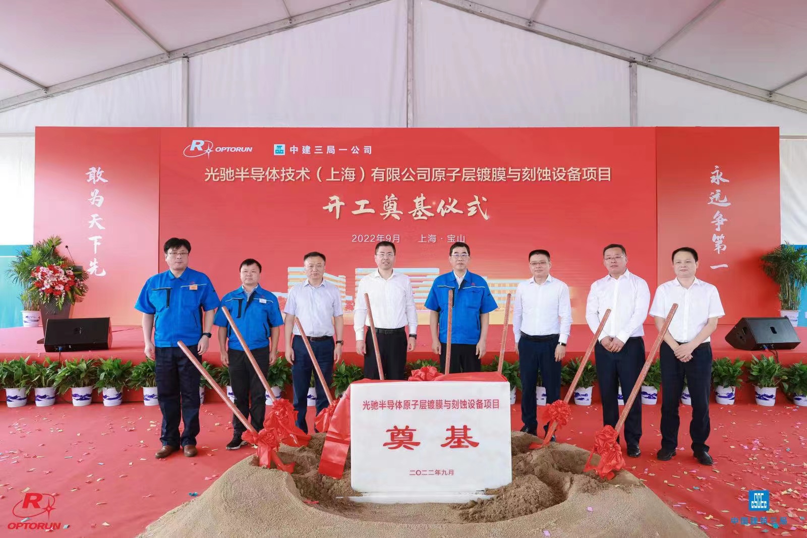

It is reported that the Guangchi Semiconductor project covers an area of 50 acres and has a total investment of 548 million yuan. It is positioned to manufacture new electronic components and equipment, and utilizes the adjustment of the global pan-semiconductor industry chain and the investment and technological integration of related cutting-edge research and development to realize the electronic special equipment manufacturing industry. It has become the innovation highland of Guangchi R&D headquarters. After the project is completed, it will have an annual production capacity of 120 high-precision atomic layer coating machines and 5 etching machines.
Guangchi Semiconductor Technology (Shanghai) Co., Ltd. is a wholly-owned subsidiary of Guangchi Technology (Shanghai) Co., Ltd. According to the official website of Guangchi Technology, the start of the project marks that the production area of Shanghai Guangchi's coating equipment has reached 53,300 square meters, which can have more manufacturing space and capacity improvement, and the product line of Guangchi has changed from traditional optics to Semiconductor optical fusion, the transformation of optical components to semiconductor integrated optics.
Here is a look at IGBT expansion and production at major Chinese fabs over the next couple of years

As you can see there. Huahong's fab 7 is going up from 18k 12-inch wpm to 25k wpm from 2021 to end of this year.
BYD Semiconductor is getting to 7k wpm by the end of this year and also have Jinan up and running by the end of this year (chart is a little off). But pretty significant that it will expand to 3 phases at Jinan. When all this complete, I think they are going 7x/8x their 2021 capacity.
Hangzhou Silan's 12 inch fab is going from producing 2k wpm in 2021 to 20k wpm by the end of this year! Huge expansion by Silan due to the expansion of auto IGBT.
CRRC's phase 2 is going from 7k 8-inch wpm to 20k by the end of this year.
From last year, the phase one max out at 10k wpm and phase two was planning to max out at 20k wpm.
On top of that, they also just announced 2 new fabs. One that is planning for 30k wpm (but could expand to 60k) for just NEVs. A second one is planning for another 30k wpm for new energy power generation, industrial control and home electronics. Huge expan plans. They are essentially planning to quadriple their IGBT capacity vs end of 2022 and 7x capacity vs end of 2021.
SMIC is a big unknown since they have quite a few new fabs along the way that will probably end up producing chips for IDMs and fabless studios. They do have the most advanced technology.
Shanghai GTA (积塔半导体) is going from just a 6-inch fab producing 15k wpm (they produce other chips also like SiC, this is just for IGBT) to adding an 8-inch fab that will produce 48k wpm. Seems like 7x/8x capacity in IGBT.
China Resources Micro (华润微) already has a fab2 in wuxi that produces 130k 8 inch wpm. Looks like from above, only a small portion of that is IGBT. It is building a new 12-inch fab in Chongqing producing 30k wpm of power chips (MOSFET, IGBT ..) That fab has just started production.
I also found another one here
Grecon semiconductor (翠展微) has some really ambitious goals. It says that there are too many orders from customers. Has huge expansion plans to meet those needs.
Although China is rapidly increasing its market share, it's still not coming close to meeting domestic needs. Although, I would say that it might be doing better than what the projection in this report is showing. As recently as 2019, it only produced 12% of domestic chips.
In 2020, Infineon had 36.5% of the world market share. Mitsubishi had 9.7% and Fuiji had 11.4%. Now, the largest Chinese player StarPower only had 2.8% market share for that year.
In 2019, Infineon had close to 50% of China's NEV market BYD was second at around 20% and StarPower was third at 16%. By the first half of this year, Infineon was down to 26% of the market based on Chinese bloggers and the big 3 domestic player for BYD/StarPower/CRRC had close to 60% of the market.
As you can see there. Huahong's fab 7 is going up from 18k 12-inch wpm to 25k wpm from 2021 to end of this year.
BYD Semiconductor is getting to 7k wpm by the end of this year and also have Jinan up and running by the end of this year (chart is a little off). But pretty significant that it will expand to 3 phases at Jinan. When all this complete, I think they are going 7x/8x their 2021 capacity.
Hangzhou Silan's 12 inch fab is going from producing 2k wpm in 2021 to 20k wpm by the end of this year! Huge expansion by Silan due to the expansion of auto IGBT.
CRRC's phase 2 is going from 7k 8-inch wpm to 20k by the end of this year.
From last year, the phase one max out at 10k wpm and phase two was planning to max out at 20k wpm.
On top of that, they also just announced 2 new fabs. One that is planning for 30k wpm (but could expand to 60k) for just NEVs. A second one is planning for another 30k wpm for new energy power generation, industrial control and home electronics. Huge expan plans. They are essentially planning to quadriple their IGBT capacity vs end of 2022 and 7x capacity vs end of 2021.
SMIC is a big unknown since they have quite a few new fabs along the way that will probably end up producing chips for IDMs and fabless studios. They do have the most advanced technology.
Shanghai GTA (积塔半导体) is going from just a 6-inch fab producing 15k wpm (they produce other chips also like SiC, this is just for IGBT) to adding an 8-inch fab that will produce 48k wpm. Seems like 7x/8x capacity in IGBT.
China Resources Micro (华润微) already has a fab2 in wuxi that produces 130k 8 inch wpm. Looks like from above, only a small portion of that is IGBT. It is building a new 12-inch fab in Chongqing producing 30k wpm of power chips (MOSFET, IGBT ..) That fab has just started production.
I also found another one here
Grecon semiconductor (翠展微) has some really ambitious goals. It says that there are too many orders from customers. Has huge expansion plans to meet those needs.
Looking to have 5% auto IGBT market (400k cars a year) by 2023 and 10% auto IGBT market (over 1 million NEVs) by 2025.翠展微规划在2023年,实现车规级IGBT模块市场的市占率达到5%,即约有40万台车搭载翠展微的IGBT模块;到2025年,市场占有率达10%,超过百万台新能源汽车搭载翠展微的IGBT模块。
Although China is rapidly increasing its market share, it's still not coming close to meeting domestic needs. Although, I would say that it might be doing better than what the projection in this report is showing. As recently as 2019, it only produced 12% of domestic chips.
In 2020, Infineon had 36.5% of the world market share. Mitsubishi had 9.7% and Fuiji had 11.4%. Now, the largest Chinese player StarPower only had 2.8% market share for that year.
In 2019, Infineon had close to 50% of China's NEV market BYD was second at around 20% and StarPower was third at 16%. By the first half of this year, Infineon was down to 26% of the market based on Chinese bloggers and the big 3 domestic player for BYD/StarPower/CRRC had close to 60% of the market.
The reason for ASML backlog orders is because of Chip Shortages especially of 28nm chips use on their EUVL and DUVL. SMIC and China wisdom on concentrating on this mature node is paying off, they may now dominate this sector as TSMC, Samsung and Intel focus on leading edge as they compete with each other on an ever smaller pie, as a result SMIC is gaining a lot of customer at their expense.
@tphuang Sir SMIC is a world leader in BCD (Bipolar-CMOS-DMOS) technology, it fit nicely with your previous post about SMIC FAB plan in Chongqing
Registered Member
SMIC met with Chongqing Municipal. ST Microelectronics and Bosch group were also there. Looks like the focus here is on auto industry and auto chips.
There is speculation that SMIC will announce new fab in Chongqing soon, since Tianjin fab was announced a month after SMIC met with the political leadership in Tianjin.
@tphuang Sir SMIC is a world leader in BCD (Bipolar-CMOS-DMOS) technology, it fit nicely with your previous post about SMIC FAB plan in Chongqing
tphuang
Brigadier
VIP ProfessionalRegistered Member
SMIC met with Chongqing Municipal. ST Microelectronics and Bosch group were also there. Looks like the focus here is on auto industry and auto chips.
There is speculation that SMIC will announce new fab in Chongqing soon, since Tianjin fab was announced a month after SMIC met with the political leadership in Tianjin.
1.5K views3 hours ago
- Status
- Not open for further replies.