Chinese semiconductor industry

Status
Not open for further replies.

hvpc

Junior Member
Registered Member
I think that is with EUV tools. Maybe because more dies are needed for a single chiplet, so to have the same productivity more EUV tools are needed. My guess is that Low NA EUV tools are not as "productive" as immersion tools......yet.
I couldn't follow what you said. Could you elaborate your reasoning?

And what is the context of the comparison table you provided? It says, "foundry cost", and the only difference is in the litho cost. Isn't that grossly/overly simplistic take on the difference?
 
Last edited:

hvpc

Junior Member
Registered Member
This question might be very simplistic, but what range of speeds in terms of GHz and what magnitude of memory in terms of GB, can 90nm microprocessor and memory chips respectively deliver?
clock speed is not the only attribute that improved from shrinking of design nodes. I think the most recent CPU clock speed has not changed much with 5nm from chips made w/ 90nm node process.

not sure why you ask, but to answer your question at face value: 90nm logic node was introduced around 2003, so that's like Pentium 4 time frame. I looked up Pentium 4, and the clock speed is like 1.3 to 3.8Ghz.

Back then the DRAM node and logic nodes have not diverged yet. For 90nm DRAM node back then, typical or most common DRAM size is 256MB and at the cusp of moving to 512MB. Common DRAM size now is 16 to 32GB. Also note, back then we are talking about 8F2 DRAM, now DRAM is made with 6F2 layout so we can pack more bits in at the same minimum feature size.
 
Last edited:

hvpc

Junior Member
Registered Member
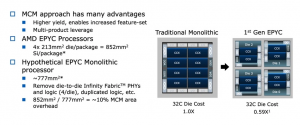
So for 5nm, the chiplet approach would be 25% more expensive than with EUV?
I think this table compares cost of foundry but not cost of chips. but even then, I question if the foundry fab cost comparison is done correctly.

to compare chip cost of monolithic vs chiplet, you have to consider the yield. Yield is inversely proportional to the die area. Larger chip area, one defect kills the entire chip. So breaking it down to multiple smaller area chips will end up with higher yield or overall lower cost. For that reason, one big 5nm monolithic chip will cost more than a chiplet made up of, say, four smaller 5nm chips.

AMD claims 41% savings between monolithic & chiplet approach.

1656767604916.png
 

hvpc

Junior Member
Registered Member
Micron's 3D NAND sector may find it very difficult to recover.

I don't see their technical advantage vs. YMTC. End user performance metrics are similar based on this teardown analysis.

Please, Log in or Register to view URLs content!

DeviceYMTC 128L XtackingSamsung 128L V-NANDMicron 128L CuA CTFSK hynix 128L 4D PUC
Parent Product (Example)Asgard PCIe4.0 NVMe1.4
AN4 1TB SSD
Samsung EVO 870 1TBMicron Crucial BX500
2.5 SSD 480GB
SK hynix Gold P31
SSD 1TB
Package MarkingsYMN09TC1B1H6CK9DVGY8J5B-DCK0OYD2D NW987H25T2TB88E
Die MarkingsCDT1BK9AHGD8J0BB37RH25TFB0
MLC OperationTLCTLCTLCTLC
ArchitectureXtackingV-NANDCTF CuA4D PUC
Number of Dice/Device41628
Memory (/die)512 Gb512 Gb512 Gb512 Gb
Die Size60.42 mm274.09 mm266.02 mm263.00 mm2
Memory Density8.48 mm26.91 mm27.76 mm28.13 mm2

As you see, YMTC 128 is the densest (512 GB per die, but smallest die). If prices are even comparable (they won't be, China always does it cheaper) then YMTC's product is superior to Micron.
This is not even the right way to compare their business' competitiveness. Yes on the surface it sure look like YMTC is more advanced. Typically, better memory density = better cost function. But this is not the case here.

Memory chips are commodities and very cost sensitive. The desire to towards lower cost/performance is what drives the transition from one node to the next (more cost effective) node.

Going to the next node where bit density is higher will provide lower cost function per bit (byte) of memory. Time-to-market, yield, operational efficiency, are also important factors. So comparing YMTC 128L to Micron 128L physical attributes are pointless.

Real comparison look something like this:
- when YMTC is producing 128L, Micron is on the more cost effective 176L node
- YMTC volume is still just a fraction of Micron's. Operation cost for larger volume is usually more cost effective
- YMTC makes their chips with new equipments. Micron makes theirs with mostly fully depreciated systems.
- YMTC buys new tools that are overkill for their current needs. Micron use old systems ("recycled") from their old DRAM process
- YMTC uses the less cost effective Xtacking (marketed to be better technically because it provides better memory density), Micron still uses the CUA (CMOS under array approach). But does the ~1mm reduction in size in x & y direction improvement from Xtacking really a big deal? It's not. This is why no one is going with that approach yet. There is no technical barrier for everyone to go to "Xtacking". people chose not to do so because they could obtain similar bit density with CUA and still have good yield.

All of the above points to a higher Cost-of-business line item on YMTC's income statement as well as a lower gross margin than their peers. So where is YMTC's advantage over their competition? The name of the game in the memory segment is who makes more money.

So, you declaring Micron is not competitive compare to YMTC is just plain incorrect.

YMTC is the new kid on the block. We are trying to build ourselves up first, then we will need to improve the technical & operational efficiency to sustain a healthy competitive business model from Profit/Loss standpoint. While YMTC is still in the growth phase, let's not kid ourselves and falsely hype it to be something that its not (yet).
 

hvpc

Junior Member
Registered Member
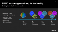
Here's latest info on Micron's 3D NAND status. These guys already have roadmap out to 4xx layers. YMTC only out to 2xx.

Below information is not to discourage, it's to show us the real gap between us and the leaders. We use this as motivation and a target to aim for. Micron is already in risk production of their 232-layer 3D NAND, moving towards HVM in a few months.

Our boys and gals at YMTC are doing a great job and accomplished much. If they could truly jump two nodes directly to 2xx layers in 2023, that's one step closer to the industry leaders.

1656771539333.png

1656771603402.png
 

xypher

Senior Member
Registered Member
Here's latest info on Micron's 3D NAND status. These guys already have roadmap out to 4xx layers. YMTC only out to 2xx.

Below information is not to discourage, it's to show us the real gap between us and the leaders. We use this as motivation and a target to aim for. Micron is already in risk production of their 232-layer 3D NAND, moving towards HVM in a few months.

Our boys and gals at YMTC are doing a great job and accomplished much. If they could truly jump two nodes directly to 2xx layers in 2023, that's one step closer to the industry leaders.

View attachment 92062


View attachment 92063
So if YMTC enters 232-layer production in 2023, then they will be on par with the leaders, not a "step closer".
 

tokenanalyst

Brigadier
Registered Member
I couldn't follow what you said. Could you elaborate your reasoning?

And what is the context of the comparison table you provided? It says, "foundry cost", and the only difference is in the litho cost. Isn't that grossly/overly simplistic take on the difference?
Yes my bad that is foundry cost per wafer. This table says that lithography cost per wafer in EUV ramps up with chiplets compared with other fab tools. But as you said chiplets require smaller dies that could have better yields and less defect than a single monolithic die so is kind of a puzzle.​

When comparing our monolithic design to the chiplet MCM design, our lithography tool time increases significantly because the
Please, Log in or Register to view URLs content!
has to be scanned 1.875 times. This is because a large part of the slit is not fully utilized. While there is still some efficiency in wafer loading time, most of the cost of a lithography tool is scan time. As a result, the internal cost per wafer has risen significantly.
In this hypothetical scenario, foundries now cost $2,174 more per wafer for lithography. That’s a huge cost increase that foundries won’t put up for high-volume customers who already have very tight margin deals. Assume that the foundry is priced by profit margin, so regardless of design, it can maintain a 50% gross margin.

The increased cost of underutilizing the slits in the reticle means that the foundry won’t sell these wafers for $17,000 to maintain a 50.2% gross margin. Instead, they will sell the wafers for $21,364. The cost of defect-free silicon for a monolithic product remains at $567. Instead of $215 per die, defect-free silicon costs $270. Instead of $430 per product, it’s $541.

The chiplet vs monolithic decision is now more difficult. Monolithic
Please, Log in or Register to view URLs content!
are likely to be cheaper to manufacture once packaging costs are factored in. Additionally, there are some power costs associated with the chiplet design. In this case, building a large monolithic chip is definitely better than using a chiplet/MCM.
Please, Log in or Register to view URLs content!

They are saying that in this case that for 5nm that cost on litho tools per wafer increase a lot.

Personally I take this with a grain of salt because there some other variables that this guys are not considering.
 

european_guy

Junior Member
Registered Member
Here's latest info on Micron's 3D NAND status. These guys already have roadmap out to 4xx layers. YMTC only out to 2xx.

Below information is not to discourage, it's to show us the real gap between us and the leaders. We use this as motivation and a target to aim for. Micron is already in risk production of their 232-layer 3D NAND, moving towards HVM in a few months.

Our boys and gals at YMTC are doing a great job and accomplished much. If they could truly jump two nodes directly to 2xx layers in 2023, that's one step closer to the industry leaders.

View attachment 92062


View attachment 92063
Thanks for this info.

I just add to your table that in May 2022 YMTC delivered samples of its new 192-layer 3D NAND flash memory to customers. Volume production is expected within year-end.

Please, Log in or Register to view URLs content!


That would be a huge result already. For instance Kioxia - Western Digital plan to start mass production of their (inferior) 162-layer 3D NAND also at the end of this year.

Please, Log in or Register to view URLs content!

So it means reducing the gap with the leaders to 1,5 - 2 years only, and closing in on Kioxia (ex Toshiba Memory) that practically invented the flash memory.
 

hvpc

Junior Member
Registered Member
So if YMTC enters 232-layer production in 2023, then they will be on par with the leaders, not a "step closer".
Touche.

But, I was also considering the delayed introduction, the slower ramp and volume in implying YMTC will not be at parity yet. Once YMTC is fully ramped to its current max capacity potential, won't happen until after 2025, and with tools fully depreciated then true-parity could be reached.
 
Status
Not open for further replies.
Top