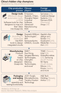
By chip packaging they could mean everything from multi-chip modules or horizontal integration, just look at how an AMD Zen 2/3 processor works for example, to vertical integration like chip stacking such as used in HBM memory, or AMD Zen 4 which uses through silicon vias. Fujitsu A64FX processor also uses advanced chip packaging technology developed by TSMC.
You are using an out of date browser. It may not display this or other websites correctly.
You should upgrade or use an alternative browser.
You should upgrade or use an alternative browser.
Chinese semiconductor industry
- Thread starter Hendrik_2000
- Start date
- Status
- Not open for further replies.
@WTAN @foofy Sir, Huawei is now investing in Lithographic machines.
from JSCh (Pakistan Defense Forum)
Hubble Technology Investment, a subsidiary of , has begun investing in the field of lithography machines and taken a stake in RSLaser Opto-Electronics Technology Co, a 193nm ArF excimer laser company that ranks No. 1 in China and No. 3 globally.
from JSCh (Pakistan Defense Forum)
Hubble Technology Investment, a subsidiary of , has begun investing in the field of lithography machines and taken a stake in RSLaser Opto-Electronics Technology Co, a 193nm ArF excimer laser company that ranks No. 1 in China and No. 3 globally.
LOL. Huawei has become an overall pain in the **s for the USA. Huawei's capital is probably beyond both SMEE and CETC. This development should accelerate the process.@WTAN @foofy Sir, Huawei is now investing in Lithographic machines.
from JSCh (Pakistan Defense Forum)
Hubble Technology Investment, a subsidiary of , has begun investing in the field of lithography machines and taken a stake in RSLaser Opto-Electronics Technology Co, a 193nm ArF excimer laser company that ranks No. 1 in China and No. 3 globally.
@BoraTas Sir, I really like to know your opinion, I read an article (check below) about Huawei filling a lithographic patent, if we connect the dot this investment is the last critical pieces to make a working prototype?LOL. Huawei has become an overall pain in the **s for the USA. Huawei's capital is probably beyond both SMEE and CETC. This development should accelerate the process.
Huawei applied for patents on lithography equipment and systems four years ago
July 22, 2020
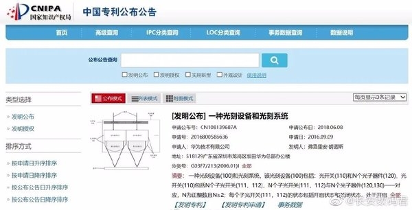
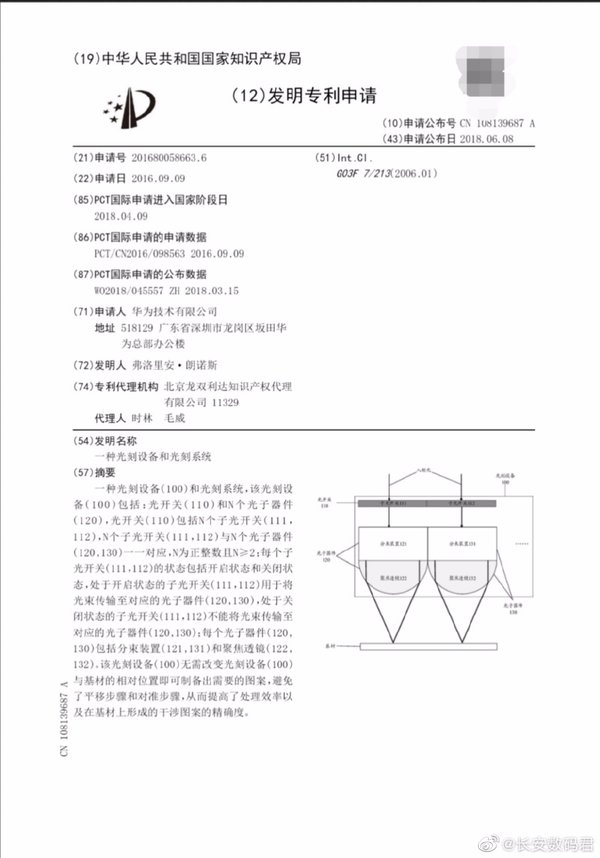
Huawei is reportedly recruiting lithography process engineers, which has sparked widespread interest. In fact, Huawei has already applied for patents for a lithography device and a lithography systems, which seem to have been prepared for the chip manufacturing process for a long time.
According to data provider Qichacha, Huawei's two patents were filed back in September 2016 and parts of them were made public in June 2018 and January 2020, respectively.
Lithography and photolithography are among the world's top technologies, and only a handful of companies worldwide have mastered the technology.

Considering that Huawei is recruiting lithography process engineers, it safe to say that Huawei does indeed have a long history of research in the chip manufacturing process.
In addition, there are reports that Huawei HiSilicon semiconductor is still in the process of expansion, is not considering scaling down.
Instead, it's actively looking for foundries to create a design and manufacturing integrated IDM.
Although Huawei HiSilicon is one of the world's top chip design companies, it is still very dependent on TSMC and a few other semiconductor companies for chip manufacturing.
Huawei's entry into the chip manufacturing field, therefore, will certainly face many difficulties, but this is also believed to be the most correct road.
It will take a long time for Huawei's IDM model to mature, and before that Huawei's various businesses will likely be looking for third-party chip supplies.
Huawei HiSilicon could have met about 80% of Huawei's mobile phone chip supply, but because of the U.S. ban, the company may have to use a lot of MediaTek chips.
Or the investment is intended for the production of photonic chips?
After Huawei's chip is banned, how to solve the problem of Chinese technology companies being caught in the chip field by foreign countries has become very critical. Although many people expect China to be completely independent of its own lithography machines and chip processes that do not rely on overseas technology, in fact, from the current technological development, China's own lithography machines have not been officially commercialized, and there is no way to talk about producing chips. . In addition, the currently independently developed lithography machine in China has only 28nm process, which is far from the current advanced process level.

This situation actually means that if the current trend continues, the domestic traditional chip manufacturing and lithography machine parts will still rely heavily on overseas technology, and companies like Huawei want It is basically impossible to rely on domestic chips to obtain chips, especially the advanced process chips that Huawei urgently needs in consumer business, which cannot be independently manufactured in China in a short time.
So in the face of this situation, domestic chip design companies have only three ways to go. The first is to hope that they will not be subject to restrictions and bans like Huawei, ZTE, and SMIC; the second is to speed up the development of domestic chip independent technology; the third is to use other technologies to replace the existing traditional chip technology and achieve Similar effect. The first path is to pin its hopes on others, which is obviously not realistic, so Huawei is currently taking the second and third paths.

Some time ago, there have been many reports that Huawei has invested in many domestic chip manufacturers. This is obviously to lay the foundation for the future. At least after China's independent chip technology has developed, it will no longer be popular. Clamp down. At the same time, Huawei itself is also working on new optical chip technology. Huawei's Wuhan optical chip factory has already begun construction and has been capped. Although there is still some distance from mass production and commercialization, Huawei clearly hopes to make optical chips. This technology is in his own hands and is not subject to bans. When this technology is further developed in the future, if Huawei's technology can achieve it, it can also be expected to get rid of the limitations of traditional lithography machines.
Speaking of optical chip technology, this silicon-based laser technology allows photonics to be more widely used in computers, and makes chip manufacturing no longer dependent on traditional lithography machines. At a time when chip technology is becoming more and more advanced and the process requirements are getting higher and higher, traditional silicon-based materials can no longer meet the process requirements. At present, the world is studying the use of carbon-based materials as materials, and there are also studies on using new photonic materials to make chips. Chips made of photonic materials are called photonic chips.

In addition to building a factory in Wuhan to develop and produce optical chips, Huawei has also recently announced a series of patents, including patents related to optical chips. The patent released by Huawei is called "Optical Computing Chip, System, and Data Processing Technology". It mainly involves an optical computing chip, system, and data processing technology, which means that Huawei will make rapid progress in AI chips.
However, it should be noted that the technical purpose of this patent published by Huawei is not simply to replace traditional chips. It is actually using optical chips to replace electric chips, realizing optical signal transmission on silicon-based materials. The real purpose of this patent is for high-precision AI chips and 5G technology. It is not the kind of future optical chip that will completely replace traditional chips on the whole. Moreover, this kind of technology is currently used in many global applications, and most of similar domestic products rely on overseas imports. At present, domestic companies that can produce high-end optical chips mainly include Haiwei Huaxin, Hisense Broadband Multimedia, Xinyisheng, Accelink Technology, Huawei HiSilicon, Huagong Technology, and Huaxi shares that entered the field of optical chips with the acquisition of Sources.

In the past, Huawei HiSilicon could also produce optical chips by itself, but compared with overseas, there is still a big gap in high-end technology, especially in the field of 25G transmitter chips, and this is why Huawei The reason for self-developed optical chips. Because these high-end products were previously imported, if they do not develop their own optical chips under the ban, then Huawei may even be restricted in AI, 5G, and other businesses that settle down.
We once again emphasize that the current optical chip manufacturer established by Huawei in Wuhan is not the kind of black technology that can replace traditional chips, as many people imagine, but a technology that has been widely used worldwide. The current high-end products of this technology are basically in the hands of overseas manufacturers. Most domestic manufacturers rely on imports for high-end optical chips and optical modules. Huawei's establishment of a factory in Wuhan is more to make up for this. Some shortcomings in the field.
Refused to be stuck! Huawei publishes patents for optical chip technology, but it does not replace traditional lithography machines
2021/06/06 22:13:59After Huawei's chip is banned, how to solve the problem of Chinese technology companies being caught in the chip field by foreign countries has become very critical. Although many people expect China to be completely independent of its own lithography machines and chip processes that do not rely on overseas technology, in fact, from the current technological development, China's own lithography machines have not been officially commercialized, and there is no way to talk about producing chips. . In addition, the currently independently developed lithography machine in China has only 28nm process, which is far from the current advanced process level.

This situation actually means that if the current trend continues, the domestic traditional chip manufacturing and lithography machine parts will still rely heavily on overseas technology, and companies like Huawei want It is basically impossible to rely on domestic chips to obtain chips, especially the advanced process chips that Huawei urgently needs in consumer business, which cannot be independently manufactured in China in a short time.
So in the face of this situation, domestic chip design companies have only three ways to go. The first is to hope that they will not be subject to restrictions and bans like Huawei, ZTE, and SMIC; the second is to speed up the development of domestic chip independent technology; the third is to use other technologies to replace the existing traditional chip technology and achieve Similar effect. The first path is to pin its hopes on others, which is obviously not realistic, so Huawei is currently taking the second and third paths.

Some time ago, there have been many reports that Huawei has invested in many domestic chip manufacturers. This is obviously to lay the foundation for the future. At least after China's independent chip technology has developed, it will no longer be popular. Clamp down. At the same time, Huawei itself is also working on new optical chip technology. Huawei's Wuhan optical chip factory has already begun construction and has been capped. Although there is still some distance from mass production and commercialization, Huawei clearly hopes to make optical chips. This technology is in his own hands and is not subject to bans. When this technology is further developed in the future, if Huawei's technology can achieve it, it can also be expected to get rid of the limitations of traditional lithography machines.
Speaking of optical chip technology, this silicon-based laser technology allows photonics to be more widely used in computers, and makes chip manufacturing no longer dependent on traditional lithography machines. At a time when chip technology is becoming more and more advanced and the process requirements are getting higher and higher, traditional silicon-based materials can no longer meet the process requirements. At present, the world is studying the use of carbon-based materials as materials, and there are also studies on using new photonic materials to make chips. Chips made of photonic materials are called photonic chips.

In addition to building a factory in Wuhan to develop and produce optical chips, Huawei has also recently announced a series of patents, including patents related to optical chips. The patent released by Huawei is called "Optical Computing Chip, System, and Data Processing Technology". It mainly involves an optical computing chip, system, and data processing technology, which means that Huawei will make rapid progress in AI chips.
However, it should be noted that the technical purpose of this patent published by Huawei is not simply to replace traditional chips. It is actually using optical chips to replace electric chips, realizing optical signal transmission on silicon-based materials. The real purpose of this patent is for high-precision AI chips and 5G technology. It is not the kind of future optical chip that will completely replace traditional chips on the whole. Moreover, this kind of technology is currently used in many global applications, and most of similar domestic products rely on overseas imports. At present, domestic companies that can produce high-end optical chips mainly include Haiwei Huaxin, Hisense Broadband Multimedia, Xinyisheng, Accelink Technology, Huawei HiSilicon, Huagong Technology, and Huaxi shares that entered the field of optical chips with the acquisition of Sources.

In the past, Huawei HiSilicon could also produce optical chips by itself, but compared with overseas, there is still a big gap in high-end technology, especially in the field of 25G transmitter chips, and this is why Huawei The reason for self-developed optical chips. Because these high-end products were previously imported, if they do not develop their own optical chips under the ban, then Huawei may even be restricted in AI, 5G, and other businesses that settle down.
We once again emphasize that the current optical chip manufacturer established by Huawei in Wuhan is not the kind of black technology that can replace traditional chips, as many people imagine, but a technology that has been widely used worldwide. The current high-end products of this technology are basically in the hands of overseas manufacturers. Most domestic manufacturers rely on imports for high-end optical chips and optical modules. Huawei's establishment of a factory in Wuhan is more to make up for this. Some shortcomings in the field.
Last edited:
Thanks for your request but my field is ASIC design automation. My knowledge about fab tools is not beyond general knowledge.@BoraTas Sir, I really like to know your opinion, I read an article (check below) about Huawei filling a lithographic patent, if we connect the dot this investment is the last critical pieces to make a working prototype?
Huawei applied for patents on lithography equipment and systems four years ago
July 22, 2020

Huawei is reportedly recruiting lithography process engineers, which has sparked widespread interest. In fact, Huawei has already applied for patents for a lithography device and a lithography systems, which seem to have been prepared for the chip manufacturing process for a long time.
According to data provider Qichacha, Huawei's two patents were filed back in September 2016 and parts of them were made public in June 2018 and January 2020, respectively.

Lithography and photolithography are among the world's top technologies, and only a handful of companies worldwide have mastered the technology.

Considering that Huawei is recruiting lithography process engineers, it safe to say that Huawei does indeed have a long history of research in the chip manufacturing process.
In addition, there are reports that Huawei HiSilicon semiconductor is still in the process of expansion, is not considering scaling down.
Instead, it's actively looking for foundries to create a design and manufacturing integrated IDM.

Although Huawei HiSilicon is one of the world's top chip design companies, it is still very dependent on TSMC and a few other semiconductor companies for chip manufacturing.
Huawei's entry into the chip manufacturing field, therefore, will certainly face many difficulties, but this is also believed to be the most correct road.
It will take a long time for Huawei's IDM model to mature, and before that Huawei's various businesses will likely be looking for third-party chip supplies.
Huawei HiSilicon could have met about 80% of Huawei's mobile phone chip supply, but because of the U.S. ban, the company may have to use a lot of MediaTek chips.
LOL. Huawei has become an overall pain in the **s for the USA. Huawei's capital is probably beyond both SMEE and CETC. This development should accelerate the process.
Huawei hires by far the most STEM graduates from top Chinese engineering schools (several dozens of universities) every year, much more than Alibbaba or Tencent or anyone else.
Huawei pays more taxes to Chinese government than any other companies every year, well, almost all (I think they're second, probably behind China Tobacco, LOL), well ahead of Alibaba or Tencent or most everybody.
Huawei R&D constitute by far the largest share of Chinese corporate R&D investments ($20+ billion a year). No other Chinese company even come to close to that amount.
I could go on to list more of those Huawei "mosts." But the above should be very indicative.
Let these facts sink in.
Yes......Huawei has made a strategic investment in Keyi Hongyuan/RS Laser. Keyi Hongyuan makes the Excimer Laser under Special Project 02 that is used in the SMEE 28nm DUVL.@WTAN @foofy Sir, Huawei is now investing in Lithographic machines.
from JSCh (Pakistan Defense Forum)
Hubble Technology Investment, a subsidiary of , has begun investing in the field of lithography machines and taken a stake in RSLaser Opto-Electronics Technology Co, a 193nm ArF excimer laser company that ranks No. 1 in China and No. 3 globally.
Huawei becomes one of the biggest Shareholders and this is a important investment.
This will allow it to influence RS lasers future strategic direction and product development.
Huawei will also arrange funds to make improvements to the existing products.
I am sure Huawei will push RS Laser to accelerate development of the CO2 Laser or any new types of Lasers for the EUVL.
Keyi Hongyuan already has future plans to develop Light Sources for the EUVL and was set up by the Chinese Academy of Sciences.
I was looking at a Popular Forum recently and came across some comments by the ASML CEO about the EUVL and China.
The ASML CEO claimed that China would be able to develop an Indigenous EUVL within 3 years.
Even the ASML CEO Peter Wennink believes this is possible in 3 years.
This is what Liberal Arts Prof. Lin Yifu of Peking University said at the forum on Future Development of Chinese Enterprises 2021.
The forum was jointly held by China Chamber of International Commerce and the National School of Development and Institute of New Structural Economics of Peking University on May 27, 2021.
According to him, ASML CEO Peter Wennink told him that he was very worried that if ASML did not sell EUV lithography systems to China now, China will soon master the technology within the next three years.
They will be then market these advanced machines to the rest of the world at very competitive prices, much lower than ASML's EUV lithography machines.
- Status
- Not open for further replies.

