Silan Micro (600460.SH) announced that the company signed the 'Strategic Cooperation Agreement for the 12-Inch High-End Analog Integrated Circuit Chip Manufacturing Production Line Project' with the Xiamen Municipal People's Government and the Haicang District People's Government of Xiamen City on October 18, 2025, in Xiamen. Additionally, the company and its wholly-owned subsidiary, Silan Micro (Xiamen), intend to increase the capital of their subsidiary, Silan Jihua, by 5.1 billion yuan together with Xiamen Semiconductor Investment Group and Xiamen Xinyi Technology Industry. Silan Jihua will act as the implementing entity for the '12-Inch High-End Analog Integrated Circuit Chip Manufacturing Production Line Project.' The project is planned to have a total investment of 20 billion yuan, with a planned production capacity of 45,000 wafers per month, implemented in two phases. Upon completion of both phases, an annual production capacity of 540,000 wafers will be established in the Haicang District of Xiamen City.
You are using an out of date browser. It may not display this or other websites correctly.
You should upgrade or use an alternative browser.
You should upgrade or use an alternative browser.
Chinese semiconductor thread II
- Thread starter vincent
- Start date
my thread on this. Just another huge mature chip project. 20B RMB is a huge investment and other countries just aren't investing in mature sector right now.
huge 32k wpm 8.6-gen AMOLED project for Visionox just got roofed. A total of 55B RMB in investment. Also got investment from Hefei govt. Just huge AMOLED capacity coming online
Last edited:
Wrong tweet?
huge 32k wpm 8.6-gen AMOLED project for Visionox just got roofed. A total of 55B RMB in investment. Also got investment from Hefei govt. Just huge AMOLED capacity coming online
Many EUV suppliers have surfaced recently.
Our target customers are primarily leading domestic and international research institutions and high-tech semiconductor companies, including the Institute of High Energy Physics (IHEP), the Institute of Optics and Fine Mechanics, the China National Space Administration (CNSA), the China Spallation Neutron Source (CSNS), the China Academy of Engineering Physics (CAEP), the Shanghai Synchrotron Radiation Facility (SSRF), and the Beijing High Energy Photon Source (BHEPS).
EUV from the Institute of Optics and Fine Mechanics, Chinese Academy of Sciences
Harbin harvesting the result of their research
Harbin Institute of Technology team! Link Technology receives angel round financing
According to Hard Krypton, LinkGen Technology recently completed an angel round of financing exceeding 10 million yuan. Investors include Qihang Investment Management's Beijing Science and Technology Development Qihang Fund and Zhongfa Xinchuang Fund, both subsidiaries of Zhongguancun Development Group. The funds will be primarily used for the research and development and industrialization of core products such as ultra-precision laser interferometers, nanoscale motion modules, and ultra-precision aperture systems, as well as to build engineering and delivery capabilities at its Shenzhen headquarters.
Link Technology was founded in December 2024 and was born based on the technological achievements of Harbin Institute of Technology. It focuses on providing ultra-precision photoelectric measurement and ultra-precision motion control products, customization and application complete solutions.

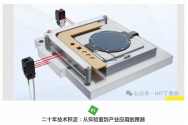
According to the official website of Lingju Technology, the company's core team originated from the Precision Instrument Engineering Research Institute of Harbin Institute of Technology. It has more than 20 years of technical accumulation in the fields of ultra-precision laser interferometer measurement technology and nano-level motion control technology. The core products independently developed by the company, such as high-speed laser interferometers, picometer-level laser interferometers, micro-probe laser interferometers, nano-level motion modules, etc., are widely used in semiconductor manufacturing, ultra-precision machining, optical assembly and adjustment, microelectronics measurement, scientific research instruments and other fields , and have been successfully delivered to dozens of domestic high-end equipment leading companies, top domestic and foreign metrology institutions , etc.

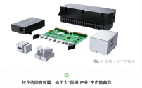
Since 2010, Harbin Institute of Technology (HIT), driven by key national science and technology projects and other core requirements, has achieved breakthroughs in key technologies such as high-speed ultra-precision motion stages and ultra-precision laser interferometers, building a comprehensive, systematic, and deep foundation in core technologies for ultra-precision instruments and equipment. The university, highly focused on the potential for industrialization of these technological achievements, actively promoted the establishment of Shenzhen Linkage and acquired a direct stake through an asset management company. The establishment of Linkage Technology will rapidly advance the transformation of high-end scientific research results into deliverable, scalable, industrial-grade products.
According to Hard Krypton, Linkage Technology has delivered over 150 systems and components to date, serving clients in the R&D, integration, and metrology and verification sectors, primarily in the areas of high-end semiconductor equipment. The company has established small-batch pilot production capabilities in Harbin, and its Shenzhen headquarters is rapidly developing local R&D and engineering teams. The company anticipates rapidly establishing a standardized, full-process design and flexible delivery system to support clients in their quest to localize critical high-end semiconductor equipment.
Last edited:
Longsys launches their new mSSD product using their latest wafer level SiP packaging and advanced heat dissipation tech.
Looks like it will support dies from different producers.
I'm surprised people are not commenting on this one more, since Lingju Tech here has already delivered 150 of its laser interferometer. That's a huge number for not just lithography, but also CNCs, optical systems & micro-electronics measurement.Harbin harvesting the result of their research
Harbin Institute of Technology team! Link Technology receives angel round financing
According to Hard Krypton, LinkGen Technology recently completed an angel round of financing exceeding 10 million yuan. Investors include Qihang Investment Management's Beijing Science and Technology Development Qihang Fund and Zhongfa Xinchuang Fund, both subsidiaries of Zhongguancun Development Group. The funds will be primarily used for the research and development and industrialization of core products such as ultra-precision laser interferometers, nanoscale motion modules, and ultra-precision aperture systems, as well as to build engineering and delivery capabilities at its Shenzhen headquarters.
Link Technology was founded in December 2024 and was born based on the technological achievements of Harbin Institute of Technology. It focuses on providing ultra-precision photoelectric measurement and ultra-precision motion control products, customization and application complete solutions.
View attachment 162900
According to the official website of Lingju Technology, the company's core team originated from the Precision Instrument Engineering Research Institute of Harbin Institute of Technology. It has more than 20 years of technical accumulation in the fields of ultra-precision laser interferometer measurement technology and nano-level motion control technology. The core products independently developed by the company, such as high-speed laser interferometers, picometer-level laser interferometers, micro-probe laser interferometers, nano-level motion modules, etc., are widely used in semiconductor manufacturing, ultra-precision machining, optical assembly and adjustment, microelectronics measurement, scientific research instruments and other fields , and have been successfully delivered to dozens of domestic high-end equipment leading companies, top domestic and foreign metrology institutions , etc.
View attachment 162899
Since 2010, Harbin Institute of Technology (HIT), driven by key national science and technology projects and other core requirements, has achieved breakthroughs in key technologies such as high-speed ultra-precision motion stages and ultra-precision laser interferometers, building a comprehensive, systematic, and deep foundation in core technologies for ultra-precision instruments and equipment. The university, highly focused on the potential for industrialization of these technological achievements, actively promoted the establishment of Shenzhen Linkage and acquired a direct stake through an asset management company. The establishment of Linkage Technology will rapidly advance the transformation of high-end scientific research results into deliverable, scalable, industrial-grade products.
According to Hard Krypton, Linkage Technology has delivered over 150 systems and components to date, serving clients in the R&D, integration, and metrology and verification sectors, primarily in the areas of high-end semiconductor equipment. The company has established small-batch pilot production capabilities in Harbin, and its Shenzhen headquarters is rapidly developing local R&D and engineering teams. The company anticipates rapidly establishing a standardized, full-process design and flexible delivery system to support clients in their quest to localize critical high-end semiconductor equipment.
I did a google search for "laser interferometer and oscilloscope" and the AI says
note, the Keysight is a competitor in laser interferometer also.A laser interferometer uses an oscilloscope to visualize the interference pattern created by laser light, allowing the user to measure distances and detect tiny vibrations. The interferometer splits a laser beam into two paths; when the beams recombine, they create a light-and-dark pattern (fringes) that is converted into an electrical signal by a photodiode. An oscilloscope displays this signal, where changes in the signal's amplitude correspond to a half-wavelength movement of the object being measured, enabling precise measurements of displacement, vibration, and other phenomena.
So, there is wide range of usage for this in not just lithography, but any advanced semiconductor equipment.
Why Interferometers Are Important in Semiconductors
Application Purpose Lithography Laser interferometers track the position of wafers with sub-nanometer precision during photolithography. Wafer Surface Inspection Measures flatness, roughness, and thickness variations using Fizeau interferometers. Film Thickness Measurement Non-contact, high-resolution measurement of thin oxide/nitride layers. Photonic Devices Used to design and test integrated optical circuits on semiconductor platforms like SOI (Silicon-on-Insulator). Stress and Strain Measurement Detects warping or thermal stress by analyzing phase shifts in interference patterns. Quantum and Sensing Applications Interferometers are foundational to high-sensitivity quantum sensors, often built on semiconductor platforms.


