Chinese semiconductor thread II

tokenanalyst

Brigadier
Registered Member

Liaoning Han Silicon Semiconductor Materials received A+ round of financing, Daohe Long-term Investment participated in the investment​

Liaoning Hangui Semiconductor Materials Co., Ltd. recently completed its A+ round of financing, and the specific amount of financing was not disclosed. Daohe Long-term Investment participated in this round of financing.
Liaoning Hansi Semiconductor Materials Co., Ltd. is located in Shenyang, Liaoning Province. It was established in 2024 and is a high-tech enterprise focusing on the field of semiconductor materials. The company's business covers the research and development, production and sales of various semiconductor materials, forming a complete industrial chain layout. Its main products include high-end materials such as silicon, silicon carbide, quartz and silicon carbide CVD coatings on various substrates.
In the field of semiconductor materials, silicon carbide, as one of the representatives of the third generation of semiconductor materials, has excellent characteristics such as wide bandgap, high breakdown electric field, and high thermal conductivity. It performs well in high temperature, high frequency, and high voltage application scenarios, and is widely used in new energy vehicles, 5G communications, smart grids, and other fields. Liaoning Hansi Semiconductor Materials Co., Ltd.'s layout in silicon carbide materials and its CVD coating technology is expected to provide more high-quality key material support for the domestic semiconductor industry chain.

Please, Log in or Register to view URLs content!
 

tokenanalyst

Brigadier
Registered Member

The application of 48V system in vehicles is accelerating, and the chip packaging solution of Changdian Technology consolidates the underlying support.​

The 48V electrical system solution for the whole vehicle (hereinafter referred to as: 48V system), with its technological innovation and multi-dimensional advantages, is gradually becoming the mainstream direction for upgrading the traditional 12V low-voltage system. At present, many OEMs are accelerating the application of 48V system solutions in mild hybrid (BHEV) and pure electric (BEV) models to meet the increasingly complex power supply needs of the new generation of models.

The 48V system can significantly enhance the power supply capacity of the vehicle, optimize the wiring harness structure and system thermal management, and support a wider range of power device selection, while maintaining the low-voltage safety standard (<60V) without adding additional high-voltage protection measures. It also improves the flexibility and adaptability of the system. Under the same power conditions, the current of the 48V system can be reduced by 1/4. This change can significantly reduce the diameter of the wire harness, reduce the amount of copper, reduce the complexity of wiring and the weight of the vehicle, while effectively reducing transmission heat loss, improving overall energy efficiency, mileage and reducing costs. Thanks to lower energy consumption, the 48V system can also reduce the CO₂ emissions of the vehicle, becoming a feasible solution for automakers to achieve energy conservation and emission reduction goals under the requirements of reducing carbon emissions. Not only that, the 48V ecosystem also has a wide range of application needs in 5G data centers, cloud computing and other fields, bringing new market opportunities.


An automotive electronics technology expert from Changdian Technology said that the 48V system solution puts forward multi-dimensional requirements for semiconductors, requiring efficient and space-saving solutions, which will drive the development of automotive semiconductors towards higher voltage resistance, higher integration and modular design, and higher reliability, and accelerate the application of new materials such as silicon carbide and gallium nitride.

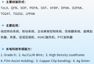
The 48V system can be divided into the power distribution end, control end, transmission end and execution end. Different chips are responsible for power management, signal control and load driving in each link to form a complete power and control system. At present, the 48V system is mainly used in high-power subsystems such as seat heaters, HVAC blowers, heat pumps, air conditioning compressors, active suspension control, wire-controlled steering, and braking systems. Its efficient power supply capability provides key support for the expansion of intelligent and electrified functions. The corresponding main chips include MOSFET, eFuse, Gate Driver, bridge driver, high-side switch and various DC/DC converters, which put forward higher requirements on power load capacity and system reliability, and pay more attention to the integration of functional safety and intelligent management.

1748879190568.png1748879212820.png

By continuously deepening its research in the field of automotive-grade packaging, Changdian Technology is able to provide 48V systems with complete packaging solutions with high reliability, and provide customers with technical support services in packaging collaborative design, simulation and packaging reliability verification, materials and performance testing, providing underlying support for driving and energy efficiency.

Compared with the traditional 12V system, the 48V architecture requires the chip to have stronger voltage carrying capacity, current handling capacity, and thermal management capabilities. Its diverse applications also require different chip packaging forms, including QFP, PDFN, SOP, SOT, DPAK, TO, etc. In terms of material selection, gold, aluminum, copper and other welding wires and copper clips are selected as interconnection materials according to different performance and functional requirements. The packaging cost is further reduced by the application of wide-row frames. In terms of process, the sintering process is used to further improve the heat dissipation performance of the device. At the same time, considering the effectiveness of space utilization, the packaging solution is also developing towards smaller size and higher integration.​


Please, Log in or Register to view URLs content!
 

tokenanalyst

Brigadier
Registered Member

Biocompatible Porphyrin Derivatives Electron Beam and Extreme Ultraviolet Photoresists: High Resolution and High Etch Resistance.​

Abstract​


Electron beam lithography (EBL) and extreme ultraviolet lithography (EUVL) have been continuously improved and applied in semiconductor and biomedical device manufacturing. With the development of biomedical nanodevices, the demand for biodegradable, and environmentally friendly materials is growing. Some biocompatible photoresists have been reported, and their sensitivity, resolution, and line edge roughness need to be further improved. In this work, porphyrin derivatives (H2TP-4Epoxy and CuTP-4Epoxy) are introduced for EBL and EUVL. Owing to their smaller sizes and higher EUV absorptivity compared to traditional polymer photoresists, CuTP-4Epoxy shows good resolution and etch resistance. As a result of EBL studies, 18 nm line/space patterns have been achieved at a dose of 1014 µC cm−2. Meanwhile, 20 nm dense patterns are also achieved using EUVL at a dose of 88.8 mJ cm−2, revealing the great potential of this approach for high resolution patterning. Etching experiments show an etch selectivity for silicon of 11.7, significantly higher than some of commercial photoresists. Biocompatibility experiments show that metalloporphyrin photoresist have potential applications in the fabrication of chips that are biocompatible with living organisms. This work demonstrates the structural advantages of porphyrin derivatives as high-resolution biocompatible photoresist materials, inspiring future exploration of metalloporphyrin materials for advanced lithography and biocompatible nanodevices.

1748881160680.png

Please, Log in or Register to view URLs content!
 

tokenanalyst

Brigadier
Registered Member

Wafer-Scale Nanoprinting of 3D Interconnects beyond Cu.​

Abstract​


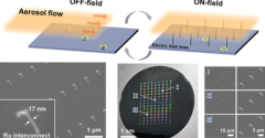
Cloud operations and services, as well as many other modern computing tasks, require hardware that is run by very densely packed integrated circuits (ICs) and heterogenous ICs. The performance of these ICs is determined by the stability and properties of the interconnects between the semiconductor devices and ICs. Although some ICs with 3D interconnects are commercially available, there has been limited progress on 3D printing utilizing emerging nanomaterials. Moreover, laying out reliable 3D metal interconnects in ICs with the appropriate electrical and physical properties remains challenging. Here, we propose high-throughput 3D interconnection with nanoscale precision by leveraging lines of forces. We successfully nanoprinted multiscale and multilevel Au, Ir, and Ru 3D interconnects on the wafer scale in non-vacuum conditions using a pulsed electric field. The ON phase of the pulsed field initiates in situ printing of nanoparticle (NP) deposition into interconnects, whereas the OFF phase allows the gas flow to evenly distribute the NPs over an entire wafer. Characterization of the 3D interconnects confirms their excellent uniformity, electrical properties, and free-form geometries, far exceeding those of any 3D-printed interconnects. Importantly, their measured resistances approach the theoretical values calculated here. The results demonstrate that 3D nanoprinting can be used to fabricate thinner and faster interconnects, which can enhance the performance of dense ICs; therefore, 3D nanoprinting can complement lithography and resolve the challenges encountered in the fabrication of critical device features.​

1748881338872.png

Please, Log in or Register to view URLs content!
 

tokenanalyst

Brigadier
Registered Member

Nano-level guardrails in ultrapure water systems: PFA fittings revolutionize semiconductor cleaning‌.​


Material Revolution: The Ultimate Barrier to Ultrapure Water Transmission

  The piping system of the semiconductor cleaning machine needs to meet the pollution control requirements of one millionth of a micron. The three characteristics of PFA material make it an irreplaceable choice:

  1. Atomic-level inert surface: The carbon-fluorine bond energy in PFA molecules is as high as 485 kJ/mol, which is more stable than ordinary plastics (CC bond 347 kJ/mol) and can resist corrosion from strong corrosive media such as hydrofluoric acid and ozone water. TSMC test data shows that after 8,000 hours of continuous operation in an acidic environment with a pH of 1, the amount of metal ions precipitated from the inner wall of the PFA joint is still less than 0.1 ppt.

  2. Ultra-smooth flow channel: The surface roughness of the PFA inner tube formed by centrifugal casting can be controlled at Ra≤0.25μm, which is 60% lower than that of traditional PTFE, effectively avoiding the retention of particles with a diameter of >0.1μm.

  3. Temperature tolerance limit: Under extreme working conditions of -196℃ liquid nitrogen cleaning to 150℃ hot DI water switching, PFA can still maintain a stable elastic modulus, and the thermal expansion coefficient (1.2×10⁻⁴/℃) is only 1/8 of that of stainless steel, avoiding micro-leakage caused by thermal stress.

1748899069034.png

On Yangtze Memory's 12-inch wafer cleaning line, the 2.3-kilometer-long PFA piping system has set a new industry benchmark:

  1. Circulation system innovation:

  The enhanced PFA bellows is used to connect the liquid storage tank and the centrifugal pump, and the anti-pulsation pressure capability is increased to 12MPa, so that the ultrapure water circulation flow rate is stabilized at 3000L/min±1%.

  2. Online monitoring breakthrough:

  Fiber Bragg gratings (FBGs) are implanted at key joints to monitor strain changes of 0.01% in real time, providing early warning of seal failure risks 48 hours in advance. After Samsung Electronics applied this technology, unplanned downtime was reduced by 72%.

  3. Energy saving and consumption reduction practices:

  The optimized 90° elbow joint reduces the pipeline pressure loss from 0.5MPa/km to 0.18MPa/km, and a single cleaning machine can save up to 42,000 kWh of electricity per year.


Future Challenges: Advancing to Atomic-Level Cleanliness


  With the popularization of processes below 3nm, PFA connectors face more stringent requirements:

  1. Breakthrough in surface energy limit: Through plasma activation treatment, the contact angle is increased from 110° to 150°, achieving the dual characteristics of "super hydrophobicity and super oleophobicity";

  2. Intelligent material iteration: Develop carbon nanotube/PFA composite materials to enable the joint to have the ability to self-sense pressure and temperature changes;

  3. Green manufacturing transformation: Develop bio-based PFA materials to reduce perfluorinated compound emissions by 90%.

Please, Log in or Register to view URLs content!
 

tokenanalyst

Brigadier
Registered Member

Wuxi Guangwei Company's ultra-high purity synthetic quartz sand project has been successfully mass-produced​


Meili Focus Wuxi Guangwei Company plans to invest a total of 200 million yuan to build three ultra-high purity quartz sand production lines. Construction will start in July 2024, and the first production line will be completed and put into production in May 2025. The annual output is expected to be 700 tons and the annual sales will be 300 million yuan. After the overall completion of the project, the annual output will increase to 2,700 tons and the annual sales will exceed 900 million yuan.

Synthetic quartz sand has good physical and chemical properties such as high hardness, high wear resistance and chemical stability. Its physical properties are similar to those of natural quartz sand, and it has good high temperature resistance, wear resistance, corrosion resistance, high compressive strength, strong insulation performance, etc. The production of synthetic quartz sand does not rely on natural quartz minerals, and can be prepared by chemical synthesis. Its technical routes include gas phase synthesis, chemical precipitation, sol-gel, silicon tetrachloride liquid phase hydrolysis, etc. Because of its higher purity and better optical properties, it is widely used in the field of high-end optics and also meets the requirements of semiconductor processes for quartz products to be high purity, pollution-free and high temperature resistant.

Please, Log in or Register to view URLs content!
 

tokenanalyst

Brigadier
Registered Member

The Institute of Microelectronics has made important scientific research progress in the field of sub-nanosecond ultrafast MRAM​


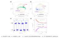
In recent years, magnetic random access memory (MRAM) has received great attention from the industry and academia due to its excellent performance. However, due to key technical bottlenecks such as the difficulty in miniaturizing the physical size to the DRAM/NAND level and the inability to reach the SRAM level in terms of writing speed (less than 1 nanosecond, or one billionth of a second), MRAM is in an awkward position in the mainstream memory market where its capacity cannot match DRAM/NAND and its speed cannot match SRAM. The fundamental physical limitation of MRAM's inability to match SRAM's writing speed is that it generates a damped spin torque through current to act on the storage layer to achieve the switching of the electrically controlled "0" and "1" states. In STT-MRAM and SOT-MRAM where the spin polarization and magnetic moment are colinear, the damped spin torque will cause the magnetic moment to precess during the "0" and "1" state transition process. This precession needs to last for 2-10 ns, limiting the writing speed of MRAM.

In response to the physical mechanism limitations of the above-mentioned writing mechanism, the 3D Memory Device and Process Research Team of the National Key Laboratory of Integrated Circuit Manufacturing Technology has discovered an ultrafast electrical writing method without magnetic moment precession and external magnetic field caused by field-like spin torque, which is expected to solve the fundamental physical problems faced by MRAM in speed and high-density integration from the source. The measured results of the device show that with a writing current one order of magnitude lower than the damped spin torque (the current STT/SOT-MRAM writing mechanism), reliable writing of the "0" and "1" states can be achieved within 200 ps (0.2 ns), and its data retention time and integration density are better than SRAM. This achievement is expected to be first applied in the fields of artificial intelligence and high-performance computing, which have stringent requirements on read and write speeds.

1748901290717.png

Please, Log in or Register to view URLs content!
 

Wahid145

Junior Member
Registered Member
Based on the development of last 5 years or so, how long do you guys think China becomes dominant in Semiconductor just like they are in EV right now?
3 to 4 years perhaps?
 
Top