Chinese semiconductor thread II

tphuang

General
Staff member
Super Moderator
VIP Professional
Registered Member

tokenanalyst

Brigadier
Registered Member

Is reported that the first GPU chip of Lisuan Technology has been packaged and successfully powered on.​

According to senior executives of Lisuan Technology, Lisuan Technology's first GPU chip has been packaged and successfully lit up.
A person familiar with the matter said, "It lit up within 24 hours after the packaging was returned."

From the first reports of operational difficulties last year, to the announcement of capital injection from investors such as listed company Dongxin Semiconductor, to the successful packaging and lighting of its products, Lisuan Technology has finally seen the light of day.
Founded in 2021, Lisuan Technology is a company that develops high-performance GPUs. It focuses on self-developed architecture and fully proprietary intellectual property rights. It has a deep understanding of the architecture, design, software development and know-how of large GPU chips, and has profound experience in processor ecosystem status and ecosystem construction.

It is reported that the founding team of Lisuan Technology has accumulated profound technical capabilities and engineering experience in the old Silicon Valley GPU company S3. Lisuan Technology co-founder and co-CEO Xuan Yifang graduated from National Chiao Tung University in Taiwan and has 28 years of GPU R&D experience. He has led the mass production of 15 generations of GPU chips; Lisuan Technology co-founder and co-CEO Kong Dehai was admitted to the undergraduate major of the Department of Radio at Tsinghua University in 1984. He has been engaged in GPU chip R&D since 1992 and is China's first generation of very large-scale integrated circuit (VLSI) designers; Lisuan Technology CTO Niu Yixin joined S3 in 1994 and is the developer of the first S3D engine and the person in charge of ViRGE, the world's first generation of 3D accelerated GPU chips. Previously, he served as the deputy general manager of GPU R&D for 18 years, leading GPU hardware design and supporting all DirectX, OpenGL, and OpenCL standards.

Please, Log in or Register to view URLs content!
 

tokenanalyst

Brigadier
Registered Member

The line will be put into operation by the end of the year! Zhuzhou CRRC 8-inch SiC production line discloses the latest progress​


On May 21, the Science and Technology Innovation Board's sub-sector collective performance briefing for the advanced rail transit industry was held at the Shanghai Stock Exchange Roadshow Center. At the meeting, Zhuzhou CRRC Times Electric Co., Ltd. exchanged views with investors on the progress of key projects and new business plans.
Li Donglin, Chairman and Executive Director of CRRC Zhuzhou, told investors that the construction of Zhuzhou Phase III will start in November 2024, and the main factory building will be topped out in May 2025. It is expected that equipment will be moved in in the second half of 2025, and the production line is expected to be completed by the end of 2025. The project is for 8-inch SiC wafers.
It is reported that Zhuzhou CRRC has a 6-inch SiC chip production line, which currently has an annual production capacity of 25,000 6-inch SiC chips.
Currently, the third-generation fine planar gate products of Zhuzhou CRRC SiC have been finalized, and the technical level is mainstream in the industry; the fourth-generation trench gate design has been finalized, reaching the advanced level in the industry, and the layout of the fifth-generation SiC technology has been completed.
At present, SiC's key products include 3300V high-voltage planar gate SiC MOSFET, 1200V fine planar gate SiC MOSFET, 1200V SBD, etc. The performance indicators of 1200V trench gate SiC MOSFET are basically comparable to those of international leading companies. At the end of 2022, the new generation of products C-Power 220s, incubated by the full SiCC-Car platform for new energy vehicles, will be officially released and are currently in the stage of sample delivery and verification by vehicle manufacturers.
Li Donglin also introduced that the company's SiC MOSFET covers 650V-6500V voltage levels, which is suitable for high-frequency/high-power density system requirements and can be widely used in new energy vehicles, UPS, wind power generation, photovoltaic inverters, railway transportation, industry, smart grids and other fields. The company's SiC products (SBD) are supplied in batches in the photovoltaic field, and SiC TO devices are supplied in batches in charging piles, OBCs, power supply detection and other fields. In 2025, the company's SiC MOSFET products are expected to break through the batch shipment of new energy vehicle main drives.

Please, Log in or Register to view URLs content!
 

tokenanalyst

Brigadier
Registered Member

Total investment of 500 million! Another semiconductor project goes into production​


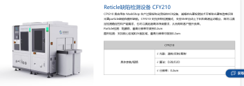
Recently, the grand ceremony of Hunan Chengfeng Mask Equipment Co., Ltd. was held in Ningxiang Economic Development Zone, Hunan Province, marking that Chengfeng Technology's strategic layout in the field of semiconductor intelligent manufacturing has entered a new stage. It is reported that the total investment of the project is 500 million yuan, mainly producing FAB front-end defect detection equipment and mask detection equipment. After the first phase is put into production, the annual output value is expected to be about 200 million yuan.

1748287488850.png
Zhuhai Chengfeng Electronic Technology Co., Ltd., is a national high-tech enterprise focusing on the research and development, production and sales of semiconductor optical inspection equipment. It has completely independent intellectual property rights, self-developed multiple sets of optical microscopy imaging technologies, and a full stack of core graphics detection algorithms that have been mastered and accumulated over many years. It can provide a full set of visual appearance defect detection solutions, which are mainly used for graphic defect detection in front-end manufacturing of semiconductor chips and back-end manufacturing of semiconductors. It has obtained more than 40 national patent technology certificates and is committed to solving the "bottleneck" problem of domestic semiconductor visual inspection, and has successfully broken the technological blockade and market monopoly of American companies.

Please, Log in or Register to view URLs content!
 

tokenanalyst

Brigadier
Registered Member

A number of major integrated circuit projects in Wuhan have made significant progress​


According to China Optics Valley, in the past two months, many integrated circuit industry chain companies such as Sunshu Technology, Cixin Technology, and Junyuan Electronics have signed contracts to settle in Optics Valley and set up R&D institutions and production lines. In the past year, Optics Valley has signed about 30 new projects worth more than 100 million yuan around the storage semiconductor industry chain, covering core equipment, components, key raw materials, EDA software, wafer manufacturing, packaging and testing, modules and other fields.

After 20 years of accumulation, from the establishment of China's first memory wafer factory in 2005, to the construction of the National Memory Base Project in 2016, to the establishment of Jiufengshan Laboratory in 2021, Optics Valley has built a "3+2" integrated circuit industry system dominated by memory semiconductors, compound semiconductors and three-dimensional integration, and featuring advanced packaging and silicon photonic integrated circuits. It is expected that the industry scale will exceed 80 billion yuan in 2024. In the field of compound semiconductors, relying on the "research-test-production" ecological system of Jiufengshan Laboratory, 30 innovative companies have landed in Optics Valley, and another 18 are in the process of transformation. At present, the construction of a number of major integrated circuit projects in Wuhan Optics Valley is being accelerated.

Please, Log in or Register to view URLs content!
 

tokenanalyst

Brigadier
Registered Member

Anjie Technology products and R&D​


Anjie Technology has deployed multiple research projects in the field of semiconductor materials, focusing on the research and development of polishing liquid, cleaning liquid, electroplating liquid and other products to meet the technical requirements of mature and advanced processes and expand market share. The total investment scale of these projects is expected to reach RMB 602,000,000, and the cumulative investment as of the end of the reporting period was RMB 746,728,100. Some projects have achieved phased results, such as stable product volume and smooth verification at the client end.

1748290225496.png
  1. Polishing liquid series products
    • Copper polishing liquid series products:The total investment is expected to be RMB 120,000,000, RMB 59,213,900 will be invested in this period, and the cumulative investment is RMB 147,667,100. Products for advanced technology nodes are steadily increasing in volume, and iterative products for mature nodes with higher cost performance have been successfully verified by multiple clients and are gradually being mass-produced and sold. The goal is to continuously develop product platforms for advanced technology nodes, optimize cost-effective products for mature technology nodes, and test and verify them on the client side, reach international advanced levels, meet the technical requirements of mature and advanced processes, and have room for growth.​
    • Barrier layer polishing liquid series products: The total investment is expected to be RMB 35,000,000, with RMB 26,904,200 invested in this period and a total investment of RMB 49,889,000. Products for advanced technology nodes are steadily increasing in volume, and iterative products for mature nodes have been successfully verified by multiple clients and gradually put into mass production and sales. The goal is to continuously develop advanced technology node product platforms, optimize mature node products, and test and verify them on the client side, reach international advanced levels, meet different process technology requirements, and expand the market.​
    • Tungsten Chemical Mechanical Polishing Slurry:The total investment is expected to be RMB 120,000,000, RMB 72,632,800 will be invested in this period, and the cumulative investment is RMB 156,465,900. Products with more advanced technology nodes are sold after verification at the client end, and products with mature technology nodes are expanded in scope of application. It is planned to continue to develop products with advanced technology nodes and test and verify them at the client end, optimize products with mature technology nodes, expand their scope of application, reach international advanced levels, meet the needs of different processes, and increase market share.​
    • Silicon substrate polishing liquid series products:The total investment is expected to be RMB 15,000,000, of which RMB 622,900 will be invested in this period, and the cumulative investment is RMB 13,755,300. The silicon polishing liquid product has been successfully verified and is gradually being mass-produced and sold. In the future, we will continue to develop and optimize the silicon polishing liquid to expand the market share, while optimizing the silicon coarse polishing liquid and verifying it on the client side to reach the international advanced level, improve the product layout, and enhance market competitiveness.​
    • Cerium Oxide Based Polishing Fluid Series: The total investment is expected to be RMB 60,000,000, with RMB 29,951,900 invested in this period and a total investment of RMB 74,966,000. Products with higher cost performance have been put into mass production and sales and continuously verified by multiple clients. Products related to advanced technology nodes have been introduced and verified and iterated by key overseas customers. The goal is to continuously develop and optimize products for mature and advanced technology nodes, conduct testing and verification on clients, expand the scope of application, reach international advanced levels, and consolidate market position.​
    • Dielectric Material Polishing Fluid Series:The total investment is expected to be RMB 12,000,000, of which RMB 6,963,800 will be invested in this period, and the cumulative investment will be RMB 10,487,600. The silicon nitride polishing liquid used in advanced logic chip process technology continues to be verified at the client end and sold in advanced memory chip technology. The silicon oxide polishing liquid gradually realizes the localization of abrasive particles, and some products have passed verification and are online. In the future, we will continue to develop and optimize silicon nitride polishing liquid, develop cost-effective silicon oxide polishing liquid and test and verify it at the client end, reach the international advanced level, and expand product applications and market share.​
    • Polishing liquid series products for new materials and new processes:The total investment is expected to be RMB 20,000,000, of which RMB 17,810,100 will be invested in this period, and the cumulative investment will be RMB 37,484,000. TSV copper/barrier polishing liquid, hybrid bonding polishing liquid, and polymer polishing liquid for three-dimensional integration process continue to be put into use by more clients as the preferred supplier, gradually expanding sales, and continuing to cooperate with advanced packaging customers to develop polishing liquid for new processes, and custom-develop polishing liquid for new materials for storage chip processes. In the future, we will continue to cooperate with customers to complete the development and testing of polishing liquids for new materials and three-dimensional integration, expand applications, reach international advanced levels, and expand market share.​

Please, Log in or Register to view URLs content!
 

tokenanalyst

Brigadier
Registered Member
  • Other Products
    • Post-etch cleaning solution:The total investment is expected to be RMB 120,000,000, of which RMB 48,992,700 will be invested in this period, and the cumulative investment is RMB 97,821,600. Products for advanced technology nodes continue to expand sales at the client end, and products requiring new technologies are continuously being developed and verified. Products for advanced technology nodes are in mass production, and iterative products with higher cost performance at mature nodes have been successfully verified at the client end and introduced into mass production. The goal is to continue to cooperate with customers to complete the development and industrialization of cleaning fluids after etching at advanced technology nodes, reach international advanced levels, improve products, and expand market share.​
    • Photoresist stripping solution:The total investment is expected to be RMB 10,000,000, of which RMB 3,062,000 will be invested in this period, and RMB 7,559,500 will be invested in total. It will be applied in batches in the fields of Beyond Moore's Law, such as wafer-level packaging, and its application will continue to expand. The products required by new technologies are continuously iterating. It aims to continuously optimize thick-film photoresist stripping liquid, meet the needs of products such as Beyond Moore's Law, reach international advanced levels, meet the needs of advanced technology nodes, and expand market prospects.​
    • Etching solution:The total investment is expected to be RMB 20,000,000, of which RMB 9,186,100 will be invested in this period, and the cumulative investment is RMB 18,776,100. The etching liquid technology platform has been successfully established, and the etching liquid has cooperated with multiple customers, and the research and development and verification are proceeding as planned. In the future, we will develop a unique formula etching liquid suitable for 12-inch advanced processes to support the development of advanced processes, reach international advanced levels, meet the needs of advanced technology nodes, and open up the market.​
    • Plating solution:The total investment is expected to be RMB 10,000,000, of which RMB 9,643,800 will be invested in this period, and the cumulative investment will be RMB 24,778,800. Improve the integrated circuit Damascus process and advanced packaging electroplating product line, and mass produce advanced packaging electroplating products. The goal is to establish an electrochemical plating technology platform, develop electroplating liquid additives that meet related processes and industrialize them, reach international advanced levels, meet the needs of integrated circuit Damascus process and advanced packaging, and expand the market.​
    • Electronic Grade Additive Purification:The total investment is expected to be RMB 30,000,000, with RMB 27,461,100 invested in this period and a total investment of RMB 54,424,300. Successfully established an electronic-grade additive purification technology platform, with multiple additives purified to ppb level and achieved stable batch production. New technology demand products are continuously being researched and verified. Aims to develop electronic-grade additive purification technology, achieve independent control of raw materials, reach international advanced levels, meet the needs of advanced technology development, and support the company's long-term development.​
    • High-end nano abrasive:The total investment is expected to be RMB 30,000,000, of which RMB 17,320,400 will be invested in this period, and the cumulative investment is RMB 52,652,900. Some products have passed the client test and verification and entered the mass production stage. The goal is to make the polishing indicators and performance reach the international advanced level, realize the complementarity of customized abrasives and imported abrasives, and ensure supply security.​
 

tokenanalyst

Brigadier
Registered Member

Naura thin film deposition revenue increased rapidly, and the equipment field blossomed in many places​


In 2024, the company's electronic process equipment revenue was 27.7 billion yuan, a year-on-year increase of 41%. Among them: 1) Etching equipment revenue exceeded 8 billion yuan, a year-on-year increase of about 33%; 2) Thin film deposition equipment revenue exceeded 10 billion yuan, a year-on-year increase of about 67%; 3) Heat treatment equipment revenue exceeded 2 billion yuan; 4) Wet process equipment revenue exceeded 1 billion yuan. In the field of etching equipment, the company has completed the layout of the full range of products including ICP, CCP, Bevel etching, high-selective etching, and dry degumming; in the field of thin film deposition, it has formed a full range of processes and equipment lineups including PVD, CVD, ALD, EPI, and ECP; the heat treatment segment covers the full range of products of vertical furnaces and rapid thermal processing (RTP); in the field of wet processes, it has built a comprehensive solution for two major systems, single-chip and slot-type.

Entering ion implantation, synergistic accumulation in multiple fields

In March 2025, the company officially announced its entry into the ion implantation equipment market and released its first ion implanter, Sirius MC 313. The company's ion implantation equipment is mainly used for the implantation of elements such as B, P, and As in 12-inch logic and memory chips. The immersion model focuses on high-dose, low-energy ion implantation, and is aimed at CMOS, hydrogenation passivation, SOI and other processes in the storage and logic fields. So far, the company has formed a closed-loop coverage of the four core links of semiconductor manufacturing equipment, which will further enhance the company's competitiveness in the domestic and foreign wafer manufacturing markets and lay a solid foundation for continuous technological innovation and domestic substitution.​
 

tokenanalyst

Brigadier
Registered Member

Looks like NAURA is researching and working upgrading their tools to support a EUV supply chain or at least support China 5nm and 3nm efforts. They have strong competition from SiCarrier and AMEC.​


Preliminary research on extreme ultraviolet ( EUV ) related equipment technology : explore the key equipment technologies such as thin film deposition and etching supporting EUV lithography, break through the core processes such as EUV reflector coating deposition and high-precision pattern etching, make technical reserves for future advanced processes below 3nm, develop atomic layer deposition ( ALD ) technology for EUV optical component coating preparation, study low-damage plasma etching technology to meet the needs of nano-scale pattern processing, and face the next generation of advanced processes for logic chips and memory chips, such as 3D NAND stacking and logic device GAA transistor structure.

High-NA EUV related thin film deposition equipment : With the support of High-NA EUV lithography technology, high-purity metal thin film deposition equipment is developed to meet the atomic-level deposition requirements of High-k dielectric layers and metal gates Plasma-enhanced atomic layer deposition ( PE-ALD ) technology is used to achieve uniformity control (thickness error < 1% ) and low defect density of thin films such as Al₂O₃ and HfO₂ , which can be used for transistor gate stacking processes of logic chips below 3nm.

Looks like they also looking to get into EBL.

Electron beam lithography ( EBL ) supporting equipment
: Develop electron beam lithography front-end thin film pretreatment equipment and detection equipment to improve the exposure accuracy and yield of nano-scale graphics, study the nano-scale uniformity control of electron beam resist coating equipment, and develop stress-free thin film deposition technology to reduce graphic distortion. It will be used in small-batch high-precision manufacturing scenarios such as advanced logic chip research and development and quantum chips.

Obviously, apart from also increasing research in Advance Packaging.

Three-dimensional integration ( 3D IC ) equipment research and development
: Develop key 2.5D/3D packaging equipment, including through silicon via ( TSV ) etcher, thin film deposition equipment and bonding equipment, improve chip stacking density and interconnection reliability, optimize deep silicon etching ( DRIE ) process, achieve high aspect ratio ( >10:1 ) TSV etching, develop high-precision copper interconnect plating equipment, meet TSV filling and redistribution layer ( RDL ) preparation requirements, and apply it to advanced packaging of AI chips and high-performance computing ( HPC ) chips, such as chiplet heterogeneous integration.

Research and development of advanced packaging equipment : Breakthrough in fan-out panel-level packaging ( FOPLP ) equipment technology, develop coating, exposure, etching and detection equipment for large-size panels (such as 12 -inch panels), study ultraviolet ( UV ) curing processes and laser grooving technology, improve packaging yield and efficiency, reduce packaging costs, and be used for high-density packaging of 5G RF chips and Internet of Things ( IoT ) sensors.​
 

european_guy

Junior Member
Registered Member

In March 2025, the company officially announced its entry into the ion implantation equipment market and released its first ion implanter, Sirius MC 313.

Now we have 3 Chinese manufacturers of ion implanters: CETC, Kingstone and NAURA

That's noteworthy because ion implantation is considered difficult tech even within semi tools and until few years ago there was no ion implanter in China, it was an US stronghold of AMAT and Axcelis.

IIRC CETC has been the first to commercialize a machine around 2018/2019.
 
Top