Come on, are we going to take every announcement at face value. Remember foxconn Wisconsin. They don't have to spend 100 billion, they have to just make an announcement.TSMC to invest $100 billion in US manufacturing
The investment will contribute to building two additional advanced chipmaking facilities in Arizona — on top of the company’s existing three already in the works — and is expected to create tens of thousands of jobs. Monday’s announcement brings TSMC’s US investments to around $165 billion.
You are using an out of date browser. It may not display this or other websites correctly.
You should upgrade or use an alternative browser.
You should upgrade or use an alternative browser.
Chinese semiconductor thread II
- Thread starter vincent
- Start date
ACM Shanghai single wafer high temperature SPM equipment passed verification
ACM Semiconductor Equipment (Shanghai) Co., Ltd. (hereinafter referred to as "ACM Shanghai") a leading supplier of wafer process solutions for semiconductor front-end and advanced packaging applications, today announced that its single-wafer medium/high temperature sulfuric acid peroxide mixture (SPM) equipment has successfully passed high-volume manufacturing verification by a logic chip manufacturer.
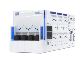
ACM Semiconductor Equipment (Shanghai) Co., Ltd. (hereinafter referred to as "ACM Shanghai") a leading supplier of wafer process solutions for semiconductor front-end and advanced packaging applications, today announced that its single-wafer medium/high temperature sulfuric acid peroxide mixture (SPM) equipment has successfully passed high-volume manufacturing verification by a logic chip manufacturer.

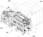
Keger Precision Machinery: Jointly applied for the invention patent of "Printing, Inspection and Labeling Machine" with Huawei, which is now in the substantive examination stage
According to the invention patent application information published by the State Intellectual Property Office, there is an invention patent application with application publication number CN119450971A, which shows that Keger Precision Machinery and Huawei jointly applied for an invention patent.
The present invention relates to the field of PCB mounting technology, and specifically discloses a printing, inspection and pasting integrated machine, including: a mainboard conveying device, used to supply the mainboard; a sub-board production line, including a sub-board feeding device for supplying the sub-board, a printing press for printing the sub-board, a printing feed conveying device for conveying the sub-board from the sub-board feeding device to the printing press, a lateral transfer manipulator for transferring the sub-board from the sub-board feeding device to the printing feed conveying device, and a printing discharge conveying device for conveying the sub-board delivered by the printing press to a printing discharge conveying device close to the mainboard conveying device; a mounting mechanism, the mounting mechanism is used to mount the sub-board on the printing discharge conveying device onto the mainboard of the mainboard conveying device. The printing, inspection and pasting integrated machine provided by the present invention can cooperate to solve the problems of low compactness of equipment structure and overly complicated production process in the existing mounting process.

Signed a contract with a top packaging factory, PrecisioNext's mass transfer technology has set off a technological revolution in wafer-level packaging and panel-level packaging
PrecisioNext Intelligence and a top packaging company have reached a strategic cooperation agreement on its mass transfer panel-level packaging equipment (FOPLP) XBonder Pro. This will be the first large-scale application of mass transfer technology in the field of IC packaging, and will set off a technological revolution in the field of wafer-level packaging and panel-level packaging. PrecisioNext is also cooperating with one of the world's leading packaging companies and a world-leading power device company on the application of XBonder Pro in wafer-level packaging.
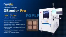
PrecisioNext Intelligence and a top packaging company have reached a strategic cooperation agreement on its mass transfer panel-level packaging equipment (FOPLP) XBonder Pro. This will be the first large-scale application of mass transfer technology in the field of IC packaging, and will set off a technological revolution in the field of wafer-level packaging and panel-level packaging. PrecisioNext is also cooperating with one of the world's leading packaging companies and a world-leading power device company on the application of XBonder Pro in wafer-level packaging.

Last edited:
Georgetown University published a study on recent semiconductor research. Results are pretty encouraging.
Key findings
- Hundreds of thousands of chip design and fabrication research papers were released between 2018 and 2023, but the field isn't growing as fast as hotter topics like AI.
- China produces by far the most chip design and fabrication research publications, with more papers from 2018-2023 than the next three countries combined.
- China also leads in top-cited chip publication output, with half of the top-cited articles featuring authors from Chinese organizations and universities.
- Most recent growth in published chip design and fabrication research came from China and India, while research output from most other countries actually shrunk over time.
Leading countries in chip design and fabrication research
Top producers of chip design and fabrication research articles, 2018-2023
Table with 4 columns and 5 rows.
�
All research Top-cited research Country Articles Country Articles China 160852 China 23520 United States 71688 United States 10300 India 39709 South Korea 3920 Japan 30401 Germany 2716 South Korea 28345 India 2706
Leading organizations in chip design and fabrication research
Top producers of chip design and fabrication research articles, 2018-2023
Table with 2 columns and 10 rows.
All research Top-cited research 1 Chinese Academy of Sciences Chinese Academy of Sciences 2 University of Chinese Academy of Sciences University of Chinese Academy of Sciences 3 Centre National de la Recherche Scientifique Tsinghua University 4 University of Electronic Science and Technology of China Nanjing University 5 Tsinghua University Huazhong University of Science and Technology 6 Nanjing University Zhejiang University 7 Xi'an Jiaotong University University of Science and Technology of China 8 Huazhong University of Science and Technology Peking University 9 Zhejiang University National University of Singapore 10 Peking University Centre National de la Recherche Scientifique
TSMC to invest $100 billion in US manufacturing
The investment will contribute to building two additional advanced chipmaking facilities in Arizona — on top of the company’s existing three already in the works — and is expected to create tens of thousands of jobs. Monday’s announcement brings TSMC’s US investments to around $165 billion.
Poof! goes Taiwan's semicon industry -- so-called "chip shield."
100 billions is not paper. They will delay as much as possible like every projects they had done in the US.Poof! goes Taiwan's semicon industry -- so-called "chip shield."
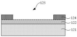
Suzhou Matrix Optoelectronics obtains patent for lithography machine exposure accuracy detection, effectively improving the spatial resolution of lithography machine exposure accuracy uniformity
Suzhou Matrix Optoelectronics Co., Ltd. obtained a patent entitled "High spatial resolution and high-precision detection method for exposure accuracy of lithography machines", with authorization announcement number CN119247707B, and the application date of December 2024.
The patent abstract shows that the present invention provides a high spatial resolution and high precision detection method for the exposure accuracy of a lithography machine, which divides the exposure area of the mask into several detection areas, and transfers the characteristic pattern to the wafer after the photolithography etching process to form several patterns on the entire wafer, and outputs an unbalanced voltage between another group of metal electrodes by inputting an electrical signal to a group of metal electrodes on the pattern, thereby drawing a Mapping diagram of the unbalanced voltage according to the coordinates of the entire wafer, and reflecting the consistency of the exposure accuracy of the lithography machine according to the distribution of the Mapping diagram. The entire exposure area of the wafer is divided into a dot matrix distribution based on the pattern, which can effectively improve the spatial resolution of the uniformity of the exposure accuracy of the lithography machine, and the smaller the pattern size, the higher the spatial resolution; in addition, through the evaluation method of the electrical performance of the pattern, the measurement accuracy of the unbalanced voltage can reach less than 1‰, achieving the purpose of high-precision detection of exposure.

Electronmicroscope analysis on Kirin 9020
The new Kirin 9020 is 140.5 mm2 -> 422 dies/wafer

Assuming a yield of 85% it means about 3.5M phones per 10K wafers, i.e. 40M phones/year, with 10K wpm of dedicated capacity.
We don't know current SMIC capacity at 7nm, it could be anything between 15K and 25K wpm or even 30Kwpm in the most optimistic case, but Kirin is only one of the many chips that SMIC has to fab at 7nm. With TSMC banned for advanced nodes, currently SMIC 7nm is a capacity bottleneck. Situation will improve when SMEE litho machines reach 7nm. The other Chinese SME players should be more or less already there.
With an investment of 12 billion yuan, the Wuhan Pioneer Rare Materials Project is expected to be fully capped in March and put into production by the end of the year
Wuhan East Lake Comprehensive Bonded Zone Pioneer Rare Materials Project, as the "key puzzle" to fill the gap in upstream semiconductor materials in Optics Valley, this industry "giant" with a planned investment of 12 billion yuan is growing rapidly at a visible speed. The project covers production workshops, R&D centers, office buildings and supporting facilities. Except for the No. 1 and No. 4 plants which are still under construction, the other main buildings have been capped in January, and it is expected that all capping will be achieved in mid-March, and the equipment installation will be completed and delivered for production before the end of the year.
Wuhan East Lake Comprehensive Bonded Zone Pioneer Rare Materials Project, as the "key puzzle" to fill the gap in upstream semiconductor materials in Optics Valley, this industry "giant" with a planned investment of 12 billion yuan is growing rapidly at a visible speed. The project covers production workshops, R&D centers, office buildings and supporting facilities. Except for the No. 1 and No. 4 plants which are still under construction, the other main buildings have been capped in January, and it is expected that all capping will be achieved in mid-March, and the equipment installation will be completed and delivered for production before the end of the year.
