Chinese semiconductor industry

Status
Not open for further replies.

tokenanalyst

Brigadier
Registered Member
JSG is a leading semiconductor material manufacturing equipments and LED substrate material manufacturing high-tech enterprise in China, which was founded in December 2006. It is the company’ mission” to build a leading semiconductor materials manufacturing equipment enterprise and develop green intelligent high-tech manufacturing industry”
1639166420741.png


Please, Log in or Register to view URLs content!
 

Jiang ZeminFanboy

Senior Member
Registered Member
What so? That's news for the semiconductor thread. And quite important. For the current lines, fabs with western tech SMIC may have problems with expanding capacity and they may be some problems in the longer period at current lines with ASML lithography, etc. before they are changed to domestic ones. SMEE, Amec, and others have their own capacity which maybe not be enough for a quick change.
 

WTAN

Junior Member
Registered Member
Excellent news.
One more nail in the coffin of ASMLs DUVL business in China.
SMIC better sue ASML to make sure that ASML provides the support for all the Lithographs that they conned SMIC into buying.
Looks like Senile Biden is carrying on the legacy of Donald Trump and Ron Vara.
This will also tech a lesson to SMIC for its obsession with Western IC Equipment.
SMIC is starting to realise that if it wants to produce advanced ICs it will have to use locally made DUVL and eventually locally made EUVL.
 

tokenanalyst

Brigadier
Registered Member
“capable of” = Means everything made in the USA, from Cymer Arf excimer lasers to Axcelis ion implanters to KlA inspection equipment to Applied materials PVD and etching equipment to synopsis EDA. There are replacement but that will required of a lot effort of Chinese companies and engineers or if the Japanese government give a damn about their semiconductor industry.

ASML -> SMEE(28nm), Nikon (desperate to revive their dying lithography business)
Applied Materials, Lam research-> Naura, Amec, TEL.
KLA, Lam research -> ACM research, Versatil, Kingsemi.
Ion Implantation-> CETC, Kingstone( They have experience with implanters for the photovoltaic industry, they can work in a high energy ion implanter for IC fabrication),Ulvac(Japan), Prema(Germany, looks like they are very oriented to the Chinese market).
Please, Log in or Register to view URLs content!

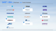
EDA->
1639180762166.png

If Chinese EDA companies are good enough for Samsung, my guess is that they will be good enough for SMIC.
 

ansy1968

Brigadier
Registered Member
@tokenanalyst ,@WTAN Sir need your opinion, I keep on seeing this news about Huawei Photonic Chip, what is its significance? Is it truly revolutionary? A way out of its current predicament? There is an excerpt in the video about a breakthrough BUT in my view it's more likely the 14nm 3D chiplet not the Photonic chip?

Please, Log in or Register to view URLs content!

Please, Log in or Register to view URLs content!

Please, Log in or Register to view URLs content!


Please, Log in or Register to view URLs content!

8 views9 minutes ago

CC
 

ansy1968

Brigadier
Registered Member
What so? That's news for the semiconductor thread. And quite important. For the current lines, fabs with western tech SMIC may have problems with expanding capacity and they may be some problems in the longer period at current lines with ASML lithography, etc. before they are changed to domestic ones. SMEE, Amec, and others have their own capacity which maybe not be enough for a quick change.
@ILikeChina bro I don't get it, next year a fully indigenous 14nm line will be introduce mass producing 14nm chips, why handicap your owned industry? Maybe a negotiating tactic, an additional leverage? See the Chinese respond, there is Non. It only gave more impetus for the Chinese IC manufacturer to go Local and make the 2025 Made in China possible.
 

tokenanalyst

Brigadier
Registered Member
@tokenanalyst ,@WTAN Sir need your opinion, I keep on seeing this news about Huawei Photonic Chip, what is its significance? Is it truly revolutionary? A way out of its current predicament? There is an excerpt in the video about a breakthrough BUT in my view it's more likely the 14nm 3D chiplet not the Photonic chip?

Please, Log in or Register to view URLs content!

Please, Log in or Register to view URLs content!

Please, Log in or Register to view URLs content!


Please, Log in or Register to view URLs content!

8 views9 minutes ago

CC

I think Huawei made an investment in the Chinese company of NanoImprint lithography called GermanLitho (not actually German) and one of the uses of NIL is photonics because unlike integrated circuits it does not require many layers and is of high resolution.

Please, Log in or Register to view URLs content!
 

ansy1968

Brigadier
Registered Member
I think Huawei made an investment in the Chinese company of NanoImprint lithography called GermanLitho (not actually German) and one of the uses of NIL is photonics because unlike integrated circuits it does not require many layers and is of high resolution.

Please, Log in or Register to view URLs content!
@tokenanalyst thanks very much bro, BUT my question is it possible? It sound to good to be true and why only China is pursuing this tech?
 
Status
Not open for further replies.
Top