Chinese semiconductor industry

Status
Not open for further replies.

BlackWindMnt

Captain
Registered Member
This forum is actually overestimated China's capabilities. China's semiconductor technologies are 10 or 15 years behind western counterpart. This is a fact.
That's the thing with China is they are always 10~15 years behind until they aren't then its all panic. China already went from 10~15 years behind in semi conductors to 5~3 years behind in a span of 3~4 years.

That the thing with fabrication in all sectors its a end to end process you might have one part like EUV handled but if you don't have the rest for sub 7nm fabrication you will not be a economically attractive semi fabricator.
 

ansy1968

Brigadier
Registered Member
That's the thing with China is they are always 10~15 years behind until they aren't then its all panic. China already went from 10~15 years behind in semi conductors to 5~3 years behind in a span of 3~4 years.

That the thing with fabrication in all sectors its a end to end process you might have one part like EUV handled but if you don't have the rest for sub 7nm fabrication you will not be a economically attractive semi fabricator.
@BlackWindMnt bro the panic turn to anger then accusation of stealing something which they don't owned, we had seen it in every sector and the disbelief is profound...lol What I'm admire about the CCP is the calmness they approach a problem, instead of complaining they work hard on the problem and work for a solution. A scientific approach worthy of praise.
 

tokenanalyst

Brigadier
Registered Member

Shanghai Xinyang: The company's ArF dry photoresist products are still under certification​

Please, Log in or Register to view URLs content!
Shanghai Xinyang said in an interaction with investors that the company's ArF dry photoresist products are still under certification. In addition, the company's ASML-1400 lithography machine and ASMLXT1900Gi lithography machine are still in the state of installation and debugging; ArF immersion photoresist products have laboratory samples and are also in the testing stage.

Regarding the issue of production capacity, Shanghai Xinyang stated that the company’s planned production capacity of KrF photoresist is 230 tons per year; the current order volume is large, but only KrF photoresist has obtained orders, and the production capacity has been fully produced according to the original plan.

Another photoresist Chinese company
 

tokenanalyst

Brigadier
Registered Member

Huawei publishes "chip package components" patent​

After the U.S. sanctions on its sanctions came into effect, Huawei, which was almost directly facing the situation of "no core available", began a series of "self-rescue" programs. International Electronic Business Information learned on the 29th that Huawei Technologies Co., Ltd. has recently disclosed the progress of a number of patent information, including a patent with the publication number CN113707623A that has attracted attention...

With the continuous development of electronic equipment in the direction of lighter, thinner, shorter and smaller, the integration of chip packaging components in electronic equipment is getting higher and higher. The industry has gradually given birth to high-density integrated embedded packaging that embeds chips in substrates or packages. Chip packaging components usually have a serious heat dissipation problem, and the heat generated by the chip cannot be effectively dissipated, which causes certain safety hazards. In response to this, in July of this year, Huawei filed a patent application entitled "Chip Packaging Components, Electronic Equipment and Manufacturing Methods of Chip Packaging Components".

1638283135903.png

Please, Log in or Register to view URLs content!
 

ansy1968

Brigadier
Registered Member

Huawei publishes "chip package components" patent​

After the U.S. sanctions on its sanctions came into effect, Huawei, which was almost directly facing the situation of "no core available", began a series of "self-rescue" programs. International Electronic Business Information learned on the 29th that Huawei Technologies Co., Ltd. has recently disclosed the progress of a number of patent information, including a patent with the publication number CN113707623A that has attracted attention...

With the continuous development of electronic equipment in the direction of lighter, thinner, shorter and smaller, the integration of chip packaging components in electronic equipment is getting higher and higher. The industry has gradually given birth to high-density integrated embedded packaging that embeds chips in substrates or packages. Chip packaging components usually have a serious heat dissipation problem, and the heat generated by the chip cannot be effectively dissipated, which causes certain safety hazards. In response to this, in July of this year, Huawei filed a patent application entitled "Chip Packaging Components, Electronic Equipment and Manufacturing Methods of Chip Packaging Components".

View attachment 79546

Please, Log in or Register to view URLs content!
@tokenanalyst bro is this related to 3D stacking chiplets?
 

gadgetcool5

Senior Member
Registered Member
I think if we consider Chinese semiconductor watching to be similar to PLA watching that we are all familiar with, then I think there is a degree of natural skepticism from English language sources who do not have intimate understanding of the Chinese language rumour base and who have done the legwork to correlate them.

I do think that relative to PLA watching, Chinese semiconductor watching is in a bit of an earlier state of maturity with a lower barrier to entry yet also with more useful information openly available... but PLA watching and the quality of "PLA analysis" or news on the PLA that most English language news media, defense journalism, and content creators put out, provides a useful starting point to treat those same analyses on Chinese semiconductors with a similar degree of skepticism.

At least, until we have a more robust system in place.
I agree with what you are saying on the informational side.

There is one major difference between PLA watching and semi watching on the other hand. For PLA watching, you tend to hope that China's best weapons are never actually forced to be used at the highest level. The J-20 is a great fighter, but I don't actually want to ever see it in a dogfight against an F-35. Why? Because that would mean China was at war with the US, which would be (IMO) a disaster. Similarly, I would never want to actually see the performance of China's hypersonic nuclear capable missiles tested in combat. These weapons do have a use, but IMO it's primarily in deterrence. It's to say: Don't mess with us because we have these weapons.

Semis on the the other hand, have a testing ground every single day: the marketplace. If you really say you have a great product, then there is a very easy acid test which is to put it out there on the market and see if anyone will buy it.

Also, I should note that it is generally underappreciated how big of a gap there is between a commercially competitive product vs. one that hits a certain node level but isn't competitive. At the latter, as the video pointed out, China has already achieved 7nm production in 2018. So the entire gap between 90nm+ and 7nm is commercialization. I feel this leads to a lot of confusion. People will say stuff like, "China can build a space station so why can't we build a lithography machine?" (Ignoring the fact that China's space station is designed to have similar parameters as the Mir space station which the Soviet Union build in the mid-1980s, and no one said Gorbachev-era USSR was a semiconductor power at the time, let alone would it be today. But that is a digression.) China's space program, like its military program, is not subject to competitive testing. You either get into space or you don't, but you don't have to be more cost effective, more efficient, and better performing than SpaceX, NASA or Roscosmos launches. There is no competition. You either achieve X or you don't. If you achieve X it's a success. But in semiconductors the issue isn't just achieving X, it's achieving X in the most efficient way, which is far, far, far harder than just achieving X. That is the difference between China's space program and its semiconductor/aviation programs. Another way to think of it is to think of a 28nm lithography machine like a car that can travel 100 miles. You can build a Model T Ford from 1914 and with a few refueling stops, say "I built a car that can travel 100 miles!" But does that mean your carmaking ability is as good as Geely or Nio today? If you put it on the marketplace, of course it won't sell.
 
Last edited:

AndrewS

Brigadier
Registered Member
I agree with what you are saying on the informational side.

There is one major difference between PLA watching and semi watching on the other hand. For PLA watching, you tend to hope that China's best weapons are never actually forced to be used at the highest level. The J-20 is a great fighter, but I don't actually want to ever see it in a dogfight against an F-35. Why? Because that would mean China was at war with the US, which would be (IMO) a disaster. Similarly, I would never want to actually see the performance of China's hypersonic nuclear capable missiles tested in combat. These weapons do have a use, but IMO it's primarily in deterrence. It's to say: Don't mess with us because we have these weapons.

Semis on the the other hand, have a testing ground every single day: the marketplace. If you really say you have a great product, then there is a very easy acid test which is to put it out there on the market and see if anyone will buy it.

Also, I should note that it is generally underappreciated how big of a gap there is between a commercially competitive product vs. one that hits a certain node level but isn't competitive. At the latter, as the video pointed out, China has already achieved 7nm production in 2018. So the entire gap between 90nm+ and 7nm is commercialization. I feel this leads to a lot of confusion. People will say stuff like, "China can build a space station so why can't we build a lithography machine?" (Ignoring the fact that China's space station is designed to have similar parameters as the Mir space station which the Soviet Union build in the mid-1980s, and no one said Gorbachev-era USSR was a semiconductor power at the time, let alone would it be today. But that is a digression.) China's space program, like its military program, is not subject to competitive testing. You either get into space or you don't, but you don't have to be more cost effective, more efficient, and better performing than SpaceX, NASA or Roscosmos launches. There is no competition. You either achieve X or you don't. If you achieve X it's a success. But in semiconductors the issue isn't just achieving X, it's achieving X in the most efficient way, which is far, far, far harder than just achieving X. That is the difference between China's space program and its semiconductor/aviation programs. Another way to think of it is to think of a 28nm lithography machine like a car that can travel 100 miles. You can build a Model T Ford from 1914 and with a few refueling stops, say "I built a car that can travel 100 miles!" But does that mean your carmaking ability is as good as Geely or Nio today? If you put it on the marketplace, of course it won't sell.

One point

Prior to SpaceX, China had the lowest space launch costs in the world

The chances are that will happen again in the future
 

tokenanalyst

Brigadier
Registered Member
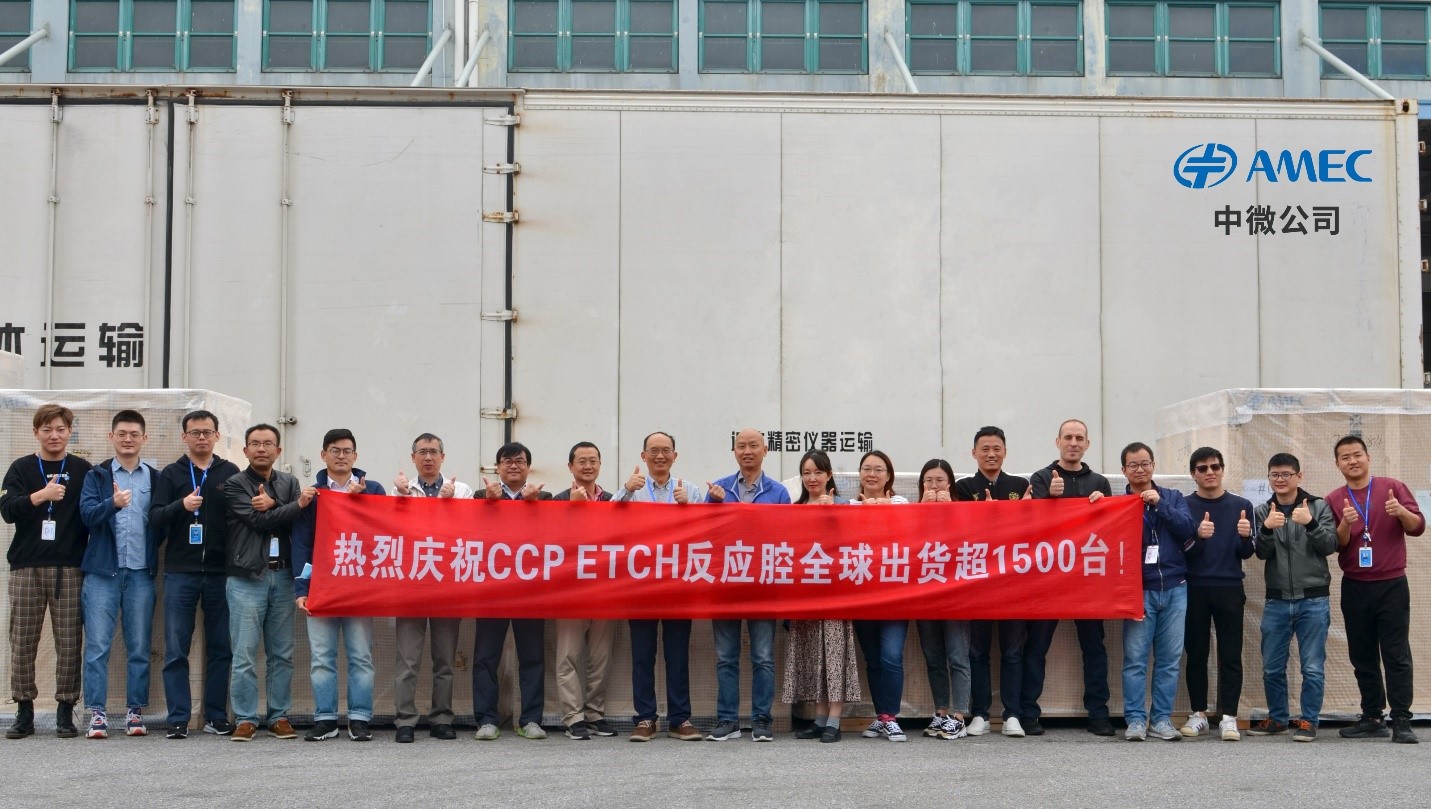
China Micro Company Celebrates the Milestone of Delivery of the 1500th CCP Etching Equipment Reaction Platform

China Micro Semiconductor Equipment (Shanghai) Co., Ltd. ushered in an important milestone on November 2, 2021: The 1500th reaction stage of China Micro Corporation’s capacitively coupled high energy plasma (CCP) etching equipment was successfully delivered to a leading domestic company Semiconductor manufacturer.

China Micro Semiconductor Equipment (Shanghai) Co., Ltd. (hereinafter referred to as "China Micro Corporation", stock code: 688012) today ushered in an important milestone: China Micro Corporation's Capacitive Coupling High Energy Plasma (CCP) etching equipment No. 1500 The two reaction stations were successfully delivered to a leading domestic semiconductor manufacturer. The Primo D-RIE® etching equipment reaction table delivered this time comes from a repeat order of the customer.

591be546025f4f26b63bef8e1e728033.jpg

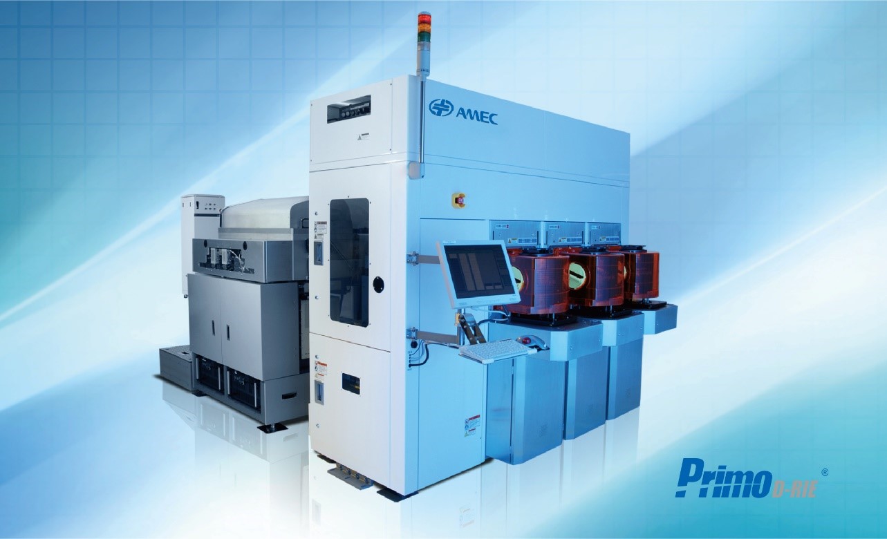
Primo D-RIE® etching equipment is used by the world's leading chip manufacturers to manufacture storage and logic devices. Customers value the advantages of this equipment in terms of stable and reliable performance, significantly improved productivity and relatively low production costs in mass production. Designed to optimize throughput, Primo D-RIE® can be configured with up to three dual-stage reaction chambers. Each reaction chamber can be operated independently and can process two wafers at the same time. In addition, the outstanding features of the equipment also include: China Micro's VHF and low frequency hybrid radio frequency decoupling reactive plasma source with independent intellectual property rights, plasma isolation ring, and advanced process components used to control the reaction environment in the cavity.

367bd61f12174a0bb5052607871ae30c.jpg

Since the release of Primo D-RIE® in 2007, China Micro Corporation has successively expanded its CCP etching equipment product line to meet the increasingly stringent technical needs of customers. In addition to Primo D-RIE® double-reaction stage etching equipment, the CCP etching equipment series also includes double-reaction stage etching equipment Primo AD-RIE®, single-reaction stage etching equipment Primo SSC AD-RIE®, Primo HD-RIE ® and Primo iDEA® that integrates etching and de-glueing. These products provide customers with comprehensive equipment solutions for a variety of applications in 5nm and below processes. China Micro's etching equipment product line also includes two other inductively coupled low energy plasma (ICP) etching equipment and through silicon via (TSV) etching equipment.
The unique innovative technology and rapidly growing market share of China Micro's plasma etching equipment have consolidated its leading position in the semiconductor front-end equipment industry at home and abroad, and promoted the company's sustainable development. So far this year, Primo HD-RIE for 3D NAND applications and Primo AD-RIE-e for logic applications at 7nm and below have accounted for 50% of total device shipments. Among them, Mainland China and Taiwan have the highest proportions. In the first three quarters of this year, China Micro's sales revenue increased by 40.4% over the same period last year, and the sales growth rate of etching equipment was about 100%.
Dr. Ni Tuqiang, Group Vice President and General Manager of Plasma Etching Products Business Headquarters of China Microelectronics, attributed this milestone of shipment and the company’s steady growth to the company’s "customer first" operating principle. He pointed out: "China Micro Innovative technology and world-class professional skills make our etching equipment products favored by leading manufacturers, and we are proud of this. Helping customers achieve their technical and profitability goals inspires everyone from the management team to the grassroots Employees, and affect every link of the entire product life cycle-from product design, equipment program customization to our professional on-site engineers to provide a full range of services. We are very grateful to our customers for their trust in Micro and Micro companies and products, we have obtained today The milestones in this year are inseparable from the long-term support of customers."
Primo D-RIE®, Primo AD-RIE®, Primo HD-RIE®, Primo SSC AD-RIE® and Primo iDEA® are registered trademarks of China Microelectronics.


Please, Log in or Register to view URLs content!
 
Status
Not open for further replies.
Top