antiterror13
Brigadier
Chinese made RAM and flash memory most likely can’t be sold in the US due to IP violations
What IPs?

Chinese made RAM and flash memory most likely can’t be sold in the US due to IP violations
American tech companies constantly sue each other for IP violations. I doubt YMTC and CXMT have deep IP portfolios to defend themselves in American courts.They can be sold. Don't spread disinformation about 337 import bans
American tech companies constantly sue each other for IP violations. I doubt YMTC and CXMT have deep IP portfolios to defend themselves in American courts.
Micron?What r u talking about? YMTC uses totally different technologies, American's IPs for NAND is minimal anyway, mostly South Korea, Japan and now China
Micron?
")
They generally settle out of court and there has been no corporate suing under Section 337 for import bans. Again, don't spread disinformationAmerican tech companies constantly sue each other for IP violations. I doubt YMTC and CXMT have deep IP portfolios to defend themselves in American courts.
Stop being so sensitive. Just telling you what will happen when products from YMTC and CXMT or products containing them get sold in the US. American companies will sue them for sure no matter they have merits or notThey generally settle out of court and there has been no corporate suing under Section 337 for import bans. Again, don't spread disinformation
@Hendrik_2000 bro that factory is owned by Foxconn? after browsing the Pakistan Defense Forum I see this.Via Vincent seem like the SMEE lithograph machine is being installed in this factory
Qingdao New Core semiconductor packaging production facility started construction on April 2020 and completed on December 2020. 46 pieces of equipment have moved into the facility already and on July 20 SMEE’s lithography machine for semiconductor packaging got delivered to the facility.
Test production starts in October and full production starts in December. The production line is focus on 5G and AI chips.
来源:爱集微
1天前
集微网消息,7月20日,青岛新核芯高端封测项目首台光刻工艺设备进场仪式在山东青岛西海岸新区举行,标志着该项目建设进入关键性节点,为年底投产奠定了坚实基础。

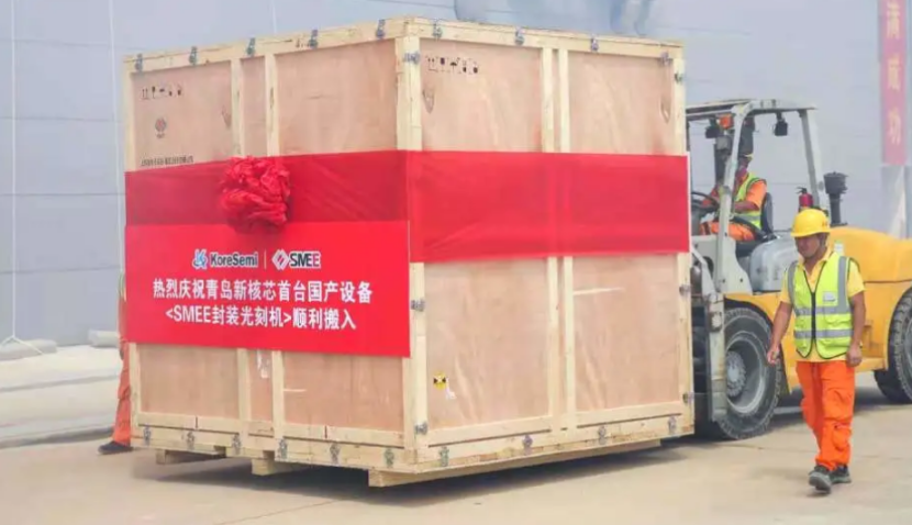
据悉,此次进场的设备为SMEE封装光刻机。
青岛西海岸新区国际招商消息显示,目前,该项目厂区已经搬入机台设备46台,预计将于10月份进行试生产,12月份形成量产能力。项目投产后将极大推动新区乃至青岛市集成电路产业转型级升,助力产业链完善,推动经济社会高质量发展。
2020年4月,青岛新核芯高端封测项目通过网上 “云签约”落地新区,将主要运用世界领先封装技术封装目前需求量快速增长的 5G通讯、人工智能等应用芯片。项目实现当年签约、当年落地、当年封顶。
2020年4月15日,青岛半导体高端封测项目通过网上“云签约”,项目落地中日(青岛)地方发展合作示范区,中日(青岛)地方发展合作示范区位于青岛西海岸新区。签约时消息显示,项目总投资10亿元,主要运用世界领先的高端封装技术,封装目前需求量快速增长的5G、人工智能等应用芯片。去年12月22日,青岛半导体高端封测项目主厂房顺利封顶。
由此看来,青岛新核芯高端封测项目或为青岛半导体高端封测项目。
Google translation
Qingdao New Core's high-end packaging and testing project enters the site, and trial production is expected in October
2205
Source: Aijiwei
1 day ago
According to the micro-network news, on July 20th, the opening ceremony of the first lithography process equipment of the Qingdao new core high-end packaging and testing project was held in the West Coast New District of Qingdao, Shandong, marking that the project has entered a key node and laid a solid foundation for the end of the year. basis.
It is reported that the equipment entering the field this time is a SMEE package lithography machine.
According to the news of international investment promotion in Qingdao West Coast New Area, 46 machines and equipment have been moved into the plant area of the project. It is expected that trial production will be carried out in October and mass production capacity will be formed in December. After the project is put into production, it will greatly promote the transformation and upgrading of the integrated circuit industry in the new district and even Qingdao, help improve the industrial chain, and promote high-quality economic and social development.
In April 2020, Qingdao's new core high-end packaging and testing project will land in the new area through online "cloud signing", and will mainly use the world's leading packaging technology to package the current rapidly growing demand for 5G communications, artificial intelligence and other application chips. The project was signed in that year, landed in that year, and capped in that year.
On April 15, 2020, the Qingdao Semiconductor High-end Packaging and Testing Project passed an online "cloud signing", and the project landed in the China-Japan (Qingdao) Local Development Cooperation Demonstration Zone. The China-Japan (Qingdao) Local Development Cooperation Demonstration Zone is located in the West Coast New District of Qingdao. According to news at the time of the contract, the project has a total investment of 1 billion yuan, mainly using the world's leading high-end packaging technology to encapsulate application chips such as 5G and artificial intelligence that are currently in rapid growth in demand. On December 22 last year, the main plant of Qingdao Semiconductor's high-end packaging and testing project was successfully topped off.
From this point of view, Qingdao's new core high-end packaging and testing project may be Qingdao Semiconductor's high-end packaging and testing project. (Proofreading/Xiaobei)