Chinese semiconductor industry

Status
Not open for further replies.

european_guy

Junior Member
Registered Member

Beijing CETC completed the delivery of 6 thinning machines​


Please, Log in or Register to view URLs content!


According to news from Jiwei.com, on June 2, 5 automatic thinning machines and 1 automatic silicon carbide thinning machine of Beijing Zhongdian Electronic Equipment Co., Ltd. (hereinafter referred to as "Beijing Zhongdian") were assembled and debugged, and met customer requirements , shipped smoothly. In addition, two dicing machines from Beijing CETC also departed on the same day.
 
Last edited:

tokenanalyst

Brigadier
Registered Member

Ultra-precision grinding below 100 microns! Enterprises in the Economic and Technological Development Zone independently research and develop silicon carbide thinning machines for mass production​


Silicon carbide thinning machine is a device for thinning silicon carbide ingots, substrate sheets or the back of chips. "Silicon carbide is a very hard material, so the accurate measurement and control of its thinning thickness is very difficult to grasp, and the requirements for the grinding accuracy of the thinning machine are very high." The relevant person in charge of Beijing Zhongdian Technology introduced that its independent The fully automatic thinning machine developed by the company solves the problem of precise thinning of silicon carbide.

1685968221692.png

This machine brings together the core components independently developed by Beijing Zhongdian Technology, such as air-floating spindle and air-floating stage, ultra-low-speed sub-micron motion control technology, and automatic control of wafer thickness by area. Good performance, strong surface precision control ability, high efficiency, small damage layer, and easy to realize automation.

Please, Log in or Register to view URLs content!
 

tokenanalyst

Brigadier
Registered Member
3.8 billion investment! North Huachuang semiconductor equipment project put into use this year

It is reported that the total investment of the semiconductor equipment industrialization base expansion project is 3.816 billion yuan, and the planned new construction area is about 365,000 square meters; the project design capacity is to produce 500 integrated circuit equipment, 500 emerging semiconductor equipment, 300 LED equipment, The production capacity of 700 sets of photovoltaic equipment.

The company's Q1 performance revenue was 3.871 billion yuan, a year-on-year increase of 81.26%; net profit attributable to the parent was 592 million yuan, a year-on-year increase of 186.58%; basic earnings per share were 1.1185 yuan. Sales orders and production scale increased compared with the same period of last year.

Please, Log in or Register to view URLs content!
 

tokenanalyst

Brigadier
Registered Member

Xinhua Semiconductor completed the B round of financing of 1 billion yuan! To fill the blank of domestic semiconductor raw material manufacturing​


Recently, Jiangsu Xinhua Semiconductor Technology Co., Ltd. (abbreviation: Xinhua Semiconductor) completed the B round of financing of 1 billion yuan. Investors include China National Building Materials New Materials Fund, CRRC Transformation Fund, CCB Investment, Pudong Science and Technology Innovation, Chengdu Science and Technology Innovation, Yuanhe Hopeful, Yuhai Capital, Hongsheng Capital and other well-known institutions.

Xinhua Semiconductor was established in 2015, jointly invested and established by Jiangsu Zhongneng Silicon Industry Technology Development Co., Ltd., which is controlled by GCL Group, and National Integrated Circuit Industry Investment Fund Co., Ltd. The main business of the company is R&D, production and sales of electronic grade polysilicon for the semiconductor industry. It is currently the only domestic enterprise that has achieved mass production of electronic grade polysilicon with full-scale coverage. In 2022, its Inner Mongolia Xinhua 10,000-ton electronic-grade polysilicon project will start construction, and it is expected to be completed and put into operation by the end of 2023.

Please, Log in or Register to view URLs content!
 

BoraTas

Captain
Registered Member
Does anyone here who is knowledgeable in the economics of the industry can tell me why Arizona was promoted by the US govt as the place for semiconductor fab projects? As everyone knows by this point semiconductor manufacturing consumes a lot of water. Last year when there was a drought in Taiwan, the Taiwanese govt had to prioritize semiconductor fabs. The effect was large enough that it became a major topic of domestic politics. Arizona is already water strained and it will only get worse. It is also far away from the talent. As a tech worker in the USA, you either work in California or New England. Texas is a distant 3rd. Why they chose Arizona?


tphuang

Lieutenant General
Staff member
Super Moderator
VIP Professional
Registered Member
However, Counterpoint expects that Huawei HiSilicon will launch its own 5G chipset in the second half of 2023. It is expected that the "N+1" node of domestic factories equivalent to TSMC's 7nm will be adopted, but since the yield rate may be lower than 50%, it is expected that the shipment in 2023 will be around 2 million to 4 million. And it is mainly aimed at the mid-end market.

Please, Log in or Register to view URLs content!

I mean < 50% is unlikely. That's way to pessimistic. Balong is going to be a pretty small chip, so I would imagine it's easier to achieve higher yield with it.

Mate 60 using Snapdragon SoC + revitalized Balong for 5G has been rumored for a while now, including from Huawei Whisper's loatest comments
下半年Mate60系列,耐心等待吧,前面提过几次了,安心等
relax, there won't be high end Kirin chip for a few more years. Even if SMIC gets really good with non-EUV 7nm process, it would be impossible for that to compete with Apple SoC. Best thing to do for HW is to stock up a lot of QCOM's latest Snapdragon chips in the likely event of a full ban

Does anyone here who is knowledgeable in the economics of the industry can tell me why Arizona was promoted by the US govt as the place for semiconductor fab projects? As everyone knows by this point semiconductor manufacturing consumes a lot of water. Last year when there was a drought in Taiwan, the Taiwanese govt had to prioritize semiconductor fabs. The effect was large enough that it became a major topic of domestic politics. Arizona is already water strained and it will only get worse. It is also far away from the talent. As a tech worker in the USA, you either work in California or New England. Texas is a distant 3rd. Why they chose Arizona?

TSMC picked it due to the tax incentives. This is another example of Asian companies coming to America without understanding of local dynamics. A lot of talented people just aren't moving out of Cali and NY.

TSMC made its own bed and should live with it rather than complaining all day.

Please, Log in or Register to view URLs content!
Also on Moore Threads, they will support direct X 11. Give them sometime. Everyone wants to see improvements, but it won't happen so quickly. They need time to improve the firmware support. It's probably easier for them to achieve those cloud desktop GPUs or even data center GPU first
 

tokenanalyst

Brigadier
Registered Member

The third-generation semiconductor compound wafer substrate project was successfully capped​

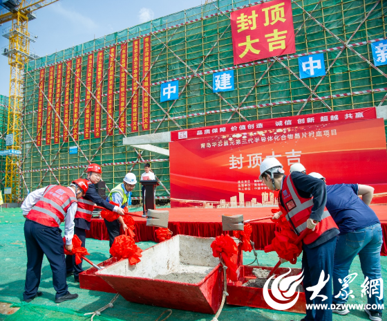
Recently, the capping ceremony of the third-generation semiconductor compound wafer substrate project undertaken by CSCEC was successfully held. Hu Xiongwei, deputy secretary and general manager of CSCEC, Zhang Yulei, manager of Shandong Branch, and leaders of Qingdao Huaxin Jingyuan Semiconductor Technology Co., Ltd. and Qingdao Commercial Construction Supervision Co., Ltd. attended the ceremony.
28833e23212abd5e152651cbd25f7a2b.png

The third-generation semiconductor compound wafer substrate project is a key project in Qingdao. After completion, it will provide important support for promoting the development of the domestic semiconductor industry and regional economic construction.
During the construction process, the project has always been adhering to the leadership of the party building, high-quality construction, the implementation of quality management process control, strict implementation of construction specifications and quality standards, and promote high-quality construction of the project.
84e8e5f561a4aff40ac6c3b8a5153994.png

The project has always adhered to high-quality construction as the core, technological innovation as the driving force, and fully promoted construction and production. Overcoming technical difficulties such as tall formwork and deep foundation pits, the 2# underground garage with a construction area of 3,669 square meters was successfully capped in only 25 days. While the project continues to promote efficient performance of the contract, it has achieved fruitful scientific and technological innovations, published 1 paper, obtained 1 patent, 1 invention patent and 1 construction method.
The project adheres to safety first and prevention first, takes safety management as the top priority of construction, strengthens the red line awareness of safety production, strictly implements the safety production responsibility system, and clearly defines the person responsible for safety production, responsible post, and responsibility area, and implements the normal state Education, training, supervision and assessment of safe production.
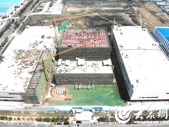
The third-generation semiconductor compound wafer substrate project is located in the north of Kehai Road, south of Keyun Road, east of Planning East Line 22, and west of Huaguan Road, Qingdao High-tech Zone, with a construction area of 62,000 square meters.

Please, Log in or Register to view URLs content!
 

KYli

Brigadier
Does anyone here who is knowledgeable in the economics of the industry can tell me why Arizona was promoted by the US govt as the place for semiconductor fab projects? As everyone knows by this point semiconductor manufacturing consumes a lot of water. Last year when there was a drought in Taiwan, the Taiwanese govt had to prioritize semiconductor fabs. The effect was large enough that it became a major topic of domestic politics. Arizona is already water strained and it will only get worse. It is also far away from the talent. As a tech worker in the USA, you either work in California or New England. Texas is a distant 3rd. Why they chose Arizona?

Arizonan state government and state universities have been lobbying for CHIPS investment and the US government subsidies for many years and are very vocal and proactive in pursuing itself as the new chip manufacturing center. Its two US senators are vital members of conservative Democrats or independent that the Biden administration needs to court.

Arizona also enjoys an advantage of its proximity to Silicon Valley. Its history of chip manufacturing is long with the SouthWest's Pioneer Semiconductor Company, Motorola and Intel all have setup chips research labs to manufacturing plants in Arizona.

Arizona also doesn't have earthquake like California. Its low property tax and cost of living are also very attractive to manufacturing companies. Its large subsidies, incentives and handouts to chips companies are probably the most important reason why TSMC chose Arizona.

Of course, Arizona also has many shortcomings such as water shortages and lack of talents. But Samsung already picked Austin, Texas. California isn't known for tax friendly and corporate friendly. New England seems to be courting smaller plants, expanding existing plants, and research labs than large plants like TSMC plants in Arizona.
 

ZeEa5KPul

Colonel
Registered Member

Beijing CETC completed the delivery of 6 thinning machines​


Please, Log in or Register to view URLs content!


According to news from Jiwei.com, on June 2, 5 automatic thinning machines and 1 automatic silicon carbide thinning machine of Beijing Zhongdian Electronic Equipment Co., Ltd. (hereinafter referred to as "Beijing Zhongdian") were assembled and debugged, and met customer requirements , shipped smoothly. In addition, two dicing machines from Beijing CETC also departed on the same day.
CETC must have shipped one of them to Mike Pompeo. Given his impressive results, I think he might have gotten two.
 
Status
Not open for further replies.
Top