Chinese semiconductor industry

Status
Not open for further replies.

FairAndUnbiased

Brigadier
Registered Member
Actually I wonder how did you find Chinese companies for specific product like this?

Japan joined chip 4 alliance
You need to understand the key parts of getting a CVD, ALD or even PVD instrument to work. Most people wouldn't think of a canister being important or how exactly precursors get delivered to a tool chamber.

When I was a TA in grad school a student complained that I solved his question by showing him a Google result. I said "if it was so easy then how come you didn't Google it yourself?" He said he didn't know what to search for. Exactly.
 

tokenanalyst

Brigadier
Registered Member

3D Heterogeneous System Integration - Technological Innovation Leads the Era of Chip Performance​


On July 5 , 2022 , by the Jinji Lake in Suzhou, at the " 10th Crystal Core Seminar -- Expanding Moore's Law : Synergistic Development Conference of Advanced Semiconductor Manufacturing and Packaging Technology " hosted by "Semiconductor Core Technology" magazine , Mr. Hong Qiyuan, Senior Vice President of SIMM Technology, gave a speech titled " Three-Dimensional Heterogeneous System Integration - Technology Innovation Leads the Era of Chip Performance". In his speech, Mr. Hong introduced the latest progress of SIMM Technology, HITOC™ technology and its 3D heterogeneous system integration business to the guests .

C:\Users\E00133\Desktop\22-7-5 tweets\9f375ca7f5a484f08f2586b3de87186.jpg


Simmon 's unique HITOC™ technology

In recent years, with the technical and cost constraints of the development of integrated circuits in various dimensions , the road along Moore's Law has become more and more rugged, and the frequency and performance of CPUs have become smaller . Advanced process node stepping. The memory wall , power consumption wall, and the limitations of advanced technology are becoming more and more pain points. The unique HITOC™ ( Heterogeneous Integration Technology on Chip ) technology of SIMM Technology enables Moore's Law to continue in the three-dimensional structure, thus leading the new track of three-dimensional chips .

C:\Users\E00110\AppData\Local\Temp\1656691730(1).png


Chipmonitor's HITOC™ technology is different from traditional advanced packaging. It uses advanced hybrid bonding (Hybrid bonding) integrated circuit manufacturing technology to integrate chips of different types , structures and even different process nodes . The most typical application scenario is to integrate the multi-functional SOC chip and the distributed DRAM chip into an ultra-high-performance single-chip . Compared with the traditional SOC with external DDR and the use of HBM-based 2.5D advanced packaging, HITOC™ technology greatly improves the performance. The density and number of connections are increased, the PHY interface is omitted, and the length of connections is greatly shortened, which can significantly reduce system power consumption and area, greatly improve storage bandwidth, and then break through memory bottlenecks, greatly enhancing the overall computing performance of the chip system. .

C:\Users\E00110\AppData\Local\Temp\1656691889(1).png


HITOC™ technology mainly includes two technical routes: Wafer-on-Wafer (wafer-to-wafer) and Die-on-Wafer (chip-to-wafer) .

Taking logic wafer to DRAM wafer as an example, after the integration of chip design and process, the logic wafer and DRAM wafer are connected together by Hybrid Bonding, and then thinned to make through -silicon vias. After the metal is drawn out and then cut and packaged, it is no different from a single chip. The chip-to-wafer technology realizes a high-performance complex chip system by bonding and stacking different chips selected by cutting and stacking on another wafer , and then through injection molding, thinning, TSV, metal wire extraction and other processes . Wafer-to-wafer technology chip products are very mature and are already in mass production. The research and development of multi- wafer-to-wafer and chip-to-wafer stacking technologies will also be basically completed by the end of this year.

As early as September 2020, SIMM Technology released the world's first high-performance AI chip based on HITOC™ architecture - SUNRISE, which has been successfully applied in the field of intelligent defect classification systems for fab production lines. At the China International Semiconductor Technology Conference (CSTIC) 2022 in June this year, Dr. Hong Feng, CEO of Corecom Technology, released the world's first VCAT 3D 4F² DRAM architecture based on HITOC™ technology. It can be seen that Chip Union Technology has innovatively used HITOC™ technology in multiple application dimensions to lead the transformation of chip products to a true three-dimensional architecture.

SIMM Technology 's 3D Heterogeneous System Integration Business

Three-dimensional heterogeneous system integration is a core business of SIMM Technology, which aims to provide customers with a complete set of three-dimensional heterogeneous system integration services in the fields of large computing power, high bandwidth, and low power consumption to enhance product value.

Simmon 's SOH™ ( System On HITOC ™ ) system integration solution can cover the entire process from chip design to mass production to help customers complete 3D heterogeneous integrated chip design and system integration , including the integration of heterogeneous integration technologies. Design consulting services, chip architecture /DFT/ mid-end and back-end solutions based on heterogeneous integration technologies, wafer / chip-level hybrid bonding design and manufacturing solutions , and related IP development and licensing business.

C:\Users\E00110\AppData\Local\Temp\1656694560(1).png


Refer to the figure above to take the three-dimensional integration of Logic + DRAM as an example:

From the chip design architecture, to the RTL, Netlist and back - end design startup , the design of Logic , DRAM , and hybrid bonding and the generation of GDS, to Logic and DRAM F ab , to Hybrid Bonding F ab Bonding production, final package testing and delivery to customers for acceptance. During the whole process, SIMM Technology can provide customers with a complete set of integrated design services based on HITOC ™ technology , including chip architecture, design, testability, back-end services and thermal simulation model solutions ; Hybrid bonding design and manufacturing solutions between multiple wafers , HITOC ™ system package test, advanced manufacturing and design consulting and training services. Of course, Simmons can also provide design services, capacity reservations and related tape-out services for Logic + DRAM , Logic + Logic and Logic + SRAM products in different stacking forms .

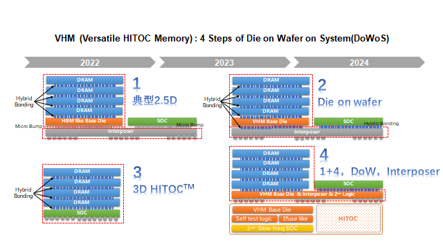
As an important part of 3D chips , Simmons can also provide related IP development and licensing services , such as VHM (Versatile HITOC ™ Memory) , HDC ( HITOC ™ DRAM Controller ) and Backside TSV , TSV , SRAM, etc. The three-dimensionalization of IP and other more heavyweight IPs is underway at the same time , and will be provided to customers one after another.

Simmons' 3D heterogeneous system integration industry ecology is very mature, and can provide customers with mature HITOC ™ 3D Design Kit , Work Flow , methodology and reference design documents. Simmons has mature and stable hybrid bonding Fab resources , as well as logic wafers and specially customizable DRAM wafer resources to meet customers' various needs from engineering verification of 3D chip architecture to mass production .
31976645.png

In addition to 3D solutions, Microcomm can also provide customers with 2.5D solutions based on VHM ( Versatile HITOC ™ Memory ) technology . Referring to the figure above, its cooperable product forms are very flexible, including:
1. HBM Like high bandwidth DRAM solution (can replace HBM and have more bandwidth and cost advantages);
2.Process in Memory solution (provides standard Memory interface, customers can customize the acceleration logic in Memory);
3.Custom SOC solution (as a co-processor and SOC packaged together to provide additional high computing power features);
4.eDRAM solution (provides a high-density high-speed storage between Last Level Cache and Main Memory).

Chipmone has successfully cooperated with a number of high-quality customers in the 3D heterogeneous system integration business. Taking Haowei Technology, a leading high-performance computing chip manufacturer , as an example, it has jointly developed with Chipmone Technology based on HITOC™ technology and will tape out in 2021 . On the successful cuckoo 2 chip, a large-capacity storage-computing integrated 3D architecture has been innovatively realized. The chip area of Cuckoo 2 reaches 800 ² . It includes multi-core, heterogeneous computing cores , Intelligent-NOC on-chip network, and a three-dimensional storage unit composed of distributed SRAM and high-bandwidth and low-latency DRAM . Its on-chip storage capacity Up to 6GBytes, memory bandwidth up to 6TB/s. A leap in performance compared to traditional architecture counterparts on the market .

Please, Log in or Register to view URLs content!
 

gelgoog

Brigadier
Registered Member
This is kind of old news about Intel. But still relevant.
Please, Log in or Register to view URLs content!

Intel Kicks Off Fab Co-Investment Program with Brookfield: New Fabs to be Jointly Owned
August 24, 2022

Intel this week introduced its new Semiconductor Co-Investment Program (SCIP) under which it will build new manufacturing facilities in collaboration with investment partners – a sharp departure from the company's traditional stance of wholly owning its logic fabs. As part of its SCIP initiative, Intel has already signed a deal with Brookfield Asset Management, which will provide Intel about $15 billion to build its fab new fab in Arizona in exchange for a 49% stake in the project. Furthermore, similar co-investment models are set to be used for other fabs in the future.
...
Under the terms of the deal, the two companies will co-invest $30 billion in the ongoing expansion of the site with Intel financing 51% and Brookfield backing 49% of the total project cost. Previously Intel planned to invest $20 billion in its Fab 52 and Fab 62, but together with Brookfield the sum has increased to $30 billion.
...
Co-ownership of semiconductor manufacturing facilities is not something unheard of the industry. China's Semiconductor Manufacturing International Co. (SMIC) invests in new fabs together with local authorities of Chinese provinces as well as various asset management companies and/or investment banks (many of which are controlled by China's federal government).
...
Yet, a co-investment program is something particularly new for Intel, which has always owned 100% of its manufacturing facilities.
 

weig2000

Captain
This is kind of old news about Intel. But still relevant.
Please, Log in or Register to view URLs content!

Intel Kicks Off Fab Co-Investment Program with Brookfield: New Fabs to be Jointly Owned
August 24, 2022

Intel this week introduced its new Semiconductor Co-Investment Program (SCIP) under which it will build new manufacturing facilities in collaboration with investment partners – a sharp departure from the company's traditional stance of wholly owning its logic fabs. As part of its SCIP initiative, Intel has already signed a deal with Brookfield Asset Management, which will provide Intel about $15 billion to build its fab new fab in Arizona in exchange for a 49% stake in the project. Furthermore, similar co-investment models are set to be used for other fabs in the future.
...
Under the terms of the deal, the two companies will co-invest $30 billion in the ongoing expansion of the site with Intel financing 51% and Brookfield backing 49% of the total project cost. Previously Intel planned to invest $20 billion in its Fab 52 and Fab 62, but together with Brookfield the sum has increased to $30 billion.
...
Co-ownership of semiconductor manufacturing facilities is not something unheard of the industry. China's Semiconductor Manufacturing International Co. (SMIC) invests in new fabs together with local authorities of Chinese provinces as well as various asset management companies and/or investment banks (many of which are controlled by China's federal government).
...
Yet, a co-investment program is something particularly new for Intel, which has always owned 100% of its manufacturing facilities.

The US is going full circle from condemning China's state capitalism to imitating Chinese practice; these include CHIPS ACT (Big Funds and state subsidies) to this Co-Investment Program (joint corporate and local government investment as practiced by SMIC, BOE, etc. for many years).
 

gelgoog

Brigadier
Registered Member
Please, Log in or Register to view URLs content!
New Zhaoxin CPU and APUs are about to launch
These links have some information about this product.
Please, Log in or Register to view URLs content!

Some quotes:
"The manufacturer's next-generation KX-6000 CPU lineup will be replacing their KX-5000 and ZX-200 CPUs which have been on the market from 2017-2018. The latest chips are expected to feature 4 cores, 8 threads, up to 3.0 GHz clock speeds, DDR4 DRAM support, PCIe 3.0 I/O, and a homegrown 16nm architecture.
...
So coming back to the Zhaoxin KX-6000G CPUs which we may as well refer to as APUs since they utilize the same Zhaoxin-made ZX C1080 GPU that is featured on the Glenfly Arise-GT-10C0 dGPU
...
According to Zhaoxin, the CPU packs 8 cores and 16 threads which is made possible through fusing two dies on the same package. The standard version of the KX-6000 CPUs only comes with the C-960 integrated GPU that offers VGA, HDMI, DP support at up to 4K resolutions.
...
For starters, in 3DMark 11, the Zhaoxin integrated GPU scores around 1000 points which is an over 3x increase compared to the older GPU.
...
While it is a huge improvement over its predecessor, the integrated chip is still only on par with an NVIDIA GT 630 graphics card in the 3DMark 11 (Performance) benchmark which scores similar points.
...
As for the CPU, the Zhaxoin (sic) chip scores over 15,000 MIPS in multi-threading decompression which puts it faster than the AMD Ryzen 3 1300X and close to Intel's Core i5-7500."

The user comments are crap though.
 

tphuang

Lieutenant General
Staff member
Super Moderator
VIP Professional
Registered Member
All these new fabs are joint venture with the local governments, including SN1/2.
Definitely. I looked this up. The amount of money that SMIC put into the JVs (documented online) are not the whole amount they said would be needed for the project. There clearly are a lot funding to be provided by local gov't. One additional way for Chinese gov't to help their domestic IC industry -> lowering the Capex and risks. Based on the expansion plan they have, there is no way their current Capex level is enough to fund all of that expansion.

They will have to search for more clients in the mainland.
Nah, China will crush them and TSMC employees will move to the mainland.

alright been busy all day at work, didn't expect this to blow up.

Your expectations is more realistic, but I think still unlikely SMIC will have 70K wpm of 14nm/7nm by 2024. With constrained WFE supply, the expected SMIC CAPEx the next few years, and timing of SN2 fab readiness, it's more likely 2026 is when SMIC could output 70K wpm. 2024/2025 for tool-move in, take some time to qualify tools, so E of 2025 or some time in 2026 to be able to turn actual capacity into actual wafer output.
so, I actually did my own estimation on this topic based on various articles I looked through. They are in this thread. Feel free to look up the sources I posted. I will start off by saying something basic. Tinrobert mentioned that each 50k wpm of 28 nm production needs 10 DUVs and each 50k wpm of 7 nm production needs 20 DUVs. I'm not in the industry, so I can't verify whether his numbers are more accurate or your number. But I would say that his numbers seemed logical based on the R&D of equipment that was discussed.

And keep in mind that the 28 nm and higher factories actually are going to be producing a lot of 45/55 nm chips and possibly even more mature than that. So, it would be a mistake for example to assume that they even need 20 DUVs for 100k wpm. Now, we do know that SMEE has already delivered SSA600 to SMIC. It's unclear to me how many were delivered and whether or not they are in use. But based on the fact that the recent news report proudly mentioned that Shanghai has the ability to mass produce 90nm lithography machines, I would imagine SMIC is getting its share of SSA600s. In general, I think it's a mistake to think they even need 20 DUVs for Beijing and Tianjin fab or 8 for Shenzhen. It seems like they are doing a lot of auto, industrial and consumer electronics chip manufacturing that do not need to Arfi machines.

And I will also say that your numbers for SN1/SN2 does not match what was announced. For example, the sources I ready said that they were spending about $9 billion Capex on SN1 with 81% of that allocated for equipment purchases. Anyway, based on the calculations I did, they were spending probably spending close to 4 times as much money on equipment purchases per 10k wpm on SN1 vs Beijing plant. Which means a few things:
1) Beijing plant is using mostly domestic machines, which are cheaper
2) Beijing plant is producing a lot of chips that are not 28 nm
3) SN1 probably received several of the latest NXT 2050i that will be used for the most advanced steps of making N+1/N+2 chips.

We also know based on a statement in the market from March of 2021 that SMIC spent enough money to buy about 20 to 25 ASML DUVs in the prior 12 months. As such, I think it's reasonable to assume that's the baseline of what they spent on a per year basis in the recent times. Given the fact that ASML is seeing mainland China as a higher % of revenue so far this year vs 2010, I would say that SMIC is likely to be buying a lot more DUVs from them. I think 30 a year is reasonable, but it's quite likely even higher than that, since Huahong really doesn't have that much capacity.

We also know that SN1 is likely close to hitting its max production of 35k wpm. Or at least, I think 25 to 30k wpm by the end of this year is probable and they likely have received the machine for this expansion in 2021. As such, the vast majority of machines they are getting this year are likely for SN2, since Shanghai Lingang plant only started construction in January of this year. I would expect Beijing plant to be getting a mix of SMEE and ASML lithography machines. Not all of which are Arfi.

Based on asml report for first half, it's likely that china bought probably 25 to 30 arfi scanners and some other scanners.

We also know that huahong announced hlmc has achieved 14 nm capabilities this year and that it's advanced node fab 6 (the only one that's doing 28 nm and more advanced) is getting close to hitting it's max capacity. So that means they are unlikely to get additional duv from asml this year. We also see that most of their expansion are in power chips and this area. While hlmc does have additional fab planned, they haven't signed any contract yet to the best of my knowledge, so will not need duvs for a couple of years.

All of which tells us:
1) SN1/SN2 aren't there to produce 14 nm chips because the capex ratio between sn1 and Beijing fab is so high.
2) Beijing, shenzhen and Tianjin plant likely have very high domestic content and are not concentrated on 28 nm node. As such, they need very few asml machines.
3) lingang fab has higher capex than Beijing, which indicate they are either more focused on 28 nm or that they will eventually also produce 14 nm node.
4) hlmc fab 6 will also produce 14 nm over the next couple of years.
5) most of duvs purchased by smic this year are likely to be installed in sn2 based on what we discussed. As such, I wouldn't be surprised if 20 asml arfi scanners this year are headed to sn2. Maybe 10 split between sn1 and Beijing pfab. 20 scanners at sn2 is enough for 35k wpm of n+2 node based on the numbers tinrobert estimated.
6) as such, I would estimate that sn1 production will be fully ramped by sometime next year and sn2 will also start production next year.
7) it is possible smic is over ordering asml arfi scanners this year in anticipation of possible sanction.
8) based on above, I would anticipate that by 2024, sn1/sn2 do not need 14nm production anymore and will fully transition to n+1 and n+2. And I would expect them to hit 70k by probably 2025. Again, the money has already been spent on asml machines. Just a matter of tuning up production. 28 to 14 nm production can be handled by other fabs of smic and huahong.
9) 70k wpm of n+1/n+2 production will allow china to produce most of its own ai, server, auto and desktop CPU/gpu. It will even allow smic to produce some lower end smartphone CPU. All of which cuts into tsmc revenue in a time of global recession. So tsmc will indeed face problems.
10) none of smic's dire warnings have slowed down their expansion plans or utilization. Same with other Chinese fabs. That's because china is far from reaching it's goal of producing 70% of own chips by 2025. Chinese fabs will be fine. Foreign chipmakers will have problems. If smic is really worried about demand, it wouldn't be fast tracking it's Tianjin fab or talking with Chongqing govt about new project.
 

tokenanalyst

Brigadier
Registered Member
These links have some information about this product.
Please, Log in or Register to view URLs content!

Some quotes:
"The manufacturer's next-generation KX-6000 CPU lineup will be replacing their KX-5000 and ZX-200 CPUs which have been on the market from 2017-2018. The latest chips are expected to feature 4 cores, 8 threads, up to 3.0 GHz clock speeds, DDR4 DRAM support, PCIe 3.0 I/O, and a homegrown 16nm architecture.
...
So coming back to the Zhaoxin KX-6000G CPUs which we may as well refer to as APUs since they utilize the same Zhaoxin-made ZX C1080 GPU that is featured on the Glenfly Arise-GT-10C0 dGPU
...
According to Zhaoxin, the CPU packs 8 cores and 16 threads which is made possible through fusing two dies on the same package. The standard version of the KX-6000 CPUs only comes with the C-960 integrated GPU that offers VGA, HDMI, DP support at up to 4K resolutions.
...
For starters, in 3DMark 11, the Zhaoxin integrated GPU scores around 1000 points which is an over 3x increase compared to the older GPU.
...
While it is a huge improvement over its predecessor, the integrated chip is still only on par with an NVIDIA GT 630 graphics card in the 3DMark 11 (Performance) benchmark which scores similar points.
...
As for the CPU, the Zhaxoin (sic) chip scores over 15,000 MIPS in multi-threading decompression which puts it faster than the AMD Ryzen 3 1300X and close to Intel's Core i5-7500."

The user comments are crap though.
It will be cool to find small form factor PCs with this CPU and GPU.
 

sunnymaxi

Captain
Registered Member
Please, Log in or Register to view URLs content!

Tech war: China chip start-ups clamour to tout AI chip breakthroughs after Nvidia sales ban, prompting analyst scepticism​

  • Chongqing-based Xiangdixian Computing Technology has unveiled Tianjun No. 1, a GPU with 12-nanometre node technology

Chinese semiconductor start-ups are rushing to claim breakthroughs in artificial intelligence (AI) chips after the US restricted the export of advanced chips from Nvidia Corp and Advanced Micro Devices (AMD) to China, prompting scepticism from many industry analysts.
Chongqing-based Xiangdixian Computing Technology, which designs microprocessors, this week unveiled Tianjun No. 1, a graphics processing unit (GPU) with 12-nanometre node technology. The company claimed it has “reached an internationally advanced level” and will “effectively fill the gap in the domestic market”, according to an official post on its WeChat account on Wednesday.

Xiangdixian, a chip design start-up founded in Chongqing, southwestern Sichuan Province in 2020, is headed by chip veteran Tang Zhimin who previously worked for Loongson Technology and Hygon Information Tech, two Chinese chip companies that make microprocessors.
 

tokenanalyst

Brigadier
Registered Member

Philosophy​

So, Van den Brink’s comments don’t point to a day of reckoning in semiconductor technology. But what about ASML itself? The prospect of the lithography roadmap ending is daunting. Without shrink, ASML will eventually cease to be an innovation-driven company and turn into a primarily cost-driven enterprise. It would become a mere shadow of its former self.

Former CEO Eric Meurice once told me that ASML’s raison d’être is lithography. Despite diversifying into metrology and other yield-enhancing technologies over the past decade, it’s fair to say that the company has stuck to that philosophy. Not that it had much choice in the matter. Every pair of hands was needed for the core business.

In the next ten years, however, I suspect we’ll see more diversification from ASML. It might not even shy away from venturing beyond its main focus of front-end lithography. Some of the most exciting future innovations in advanced semiconductor technology will be seen in the back-end. Perhaps that’s a good place to start looking.

Please, Log in or Register to view URLs content!

If ASML decide to enter the back end lithography market or advanced packaging or maskless lithography or NIL, everyone in those areas is doomed.
 
Status
Not open for further replies.
Top