
I don't know IF one of our esteem members had posted it before so I apologized in advance.
China’s leading IC testing company Leadyo completes world’s first 3nm chip test
Chinese article by 日新
English Editor WM Zhang

07-13 15:50
By Li Panpan
China’s leading IC testing company Leadyo(利扬芯片) said it completed the test and development of the world's first 3nm chip.
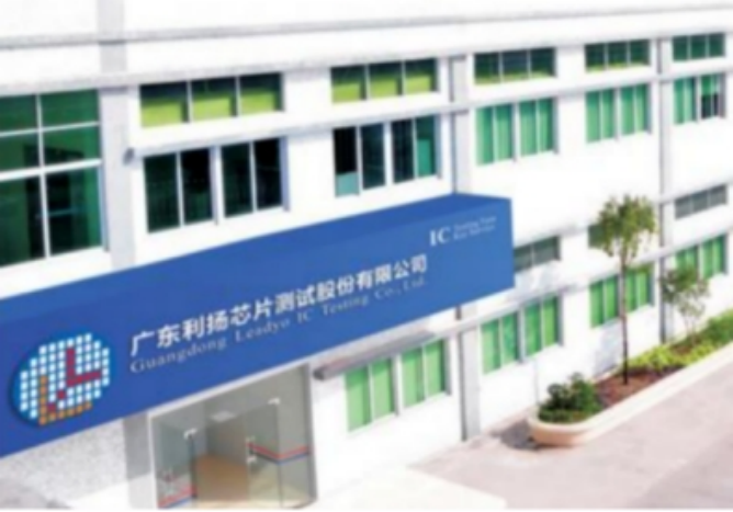
The company based in Dongguan of southern China’s Guangdong Province shared this information in its investor relationship management platform of the Shanghai Stock Exchange on July 7, saying that with rich experiences in testing 8nm and 5nm chip products, it would advance mass test of 3nm chips in an orderly manner.
Leadyo was founded in February 2010 and listed in the STR Market of Shanghai Stock Exchange in 2020. It has tested 44 categories of 12-inch and 8-inch chip products of various process technology.
It has increased investment in testing and R&D of high-end chips, especially the computing power chip testing technology, with a complete set of testing solutions for the discrete problems of advanced manufacturing processes.
Its testing solutions are widely used in chips for 5G communications, computers, consumer electronics, automotive electronics, biometrics, MCU, AIoT, and industrial control.
And Samsung is the first FAB customer to use it to mass produce their 3nm chips.
08/07/2022
Chinese semiconductor company Leadyo chip today in response to investor questions, said: the current 3nm advanced process process chip test program has been successfully debugged, marking the company completed the world’s first 3nm chip test development, will be to the mass production test phase in an orderly manner.
Q: Recently, we saw the media report that Samsung launched the world’s first 3nm chip, which is OEM for a domestic mining chip design company, does your company have the opportunity to become their test supplier?
A: In recent years, the company has been increasing its investment in high-end chip research and development, especially the company’s arithmetic chip testing technology for advanced process discrete problems to provide a full set of test solutions, focusing on solving the power consumption ratio, chip internal resistance, high-current test circuit, test temperature control and other key technical difficulties, the first 8nm and 5nm chip products for a number of customers to provide mass production test services. At present, the chip test solution for 3nm advanced process has been successfully debugged, marking the completion of the world’s first 3nm chip test development, and will advance to the mass production test stage in an orderly manner.
Samsung Electronics announced on June 30 that the company has begun mass production of 3nm semiconductor chips in its Hwaseong plant in South Korea, the world’s first company to mass produce 3nm chips. Unlike previous generations of chips using FinFETs, Samsung uses the GAA (Gate All Around) transistor architecture, which greatly improves power efficiency.
Established in February 2010, Guangdong Leadyo Chip Testing Co., Ltd. claims to be a well-known independent third-party professional chip testing technology service provider in China, a national special-purpose small giant enterprise and a high-tech enterprise, whose main business includes IC testing solution development, 12-inch and 8-inch wafer testing services, finished chip testing services and supporting services related to IC testing.
Officially, the company has been focusing on IC testing since its establishment, and has accumulated a number of independent core technologies in this field. It has developed 44 categories of chip testing solutions, which can be applied to the testing needs of different terminal application scenarios, and completed the mass production testing of more than 4,300 chip models.
In addition, the company also provides independent third-party testing services for mid-to-high-end chips for well-known chip design companies in China, with products mainly used in communications, computers, consumer electronics, automotive electronics and industrial control, covering advanced processes such as 8nm, 16nm and 28nm.
The company has not yet announced its second quarter financial results. The operating income in the first quarter increased 57.47% year-on-year, and the net profit attributable to shareholders of the listed company increased 14.69% year-on-year if excluding the impact of share-based payment on net profit from the implementation of equity incentives.
Leadyo Chip A shares once rose more than 11%, has now partially fallen back, now reported 32.58 yuan per share, market value of 4.438 billion yuan.
So at least China had a foot on the door regarding 3nm node processed, so maybe within 3 years we may see it mass produce either thru an EUVL Chinese machine or ASML advance DUVL (NXT 2100i) using nVSAFET and CFET architecture?
China’s leading IC testing company Leadyo completes world’s first 3nm chip test
Chinese article by 日新
English Editor WM Zhang
07-13 15:50
By Li Panpan
China’s leading IC testing company Leadyo(利扬芯片) said it completed the test and development of the world's first 3nm chip.
The company based in Dongguan of southern China’s Guangdong Province shared this information in its investor relationship management platform of the Shanghai Stock Exchange on July 7, saying that with rich experiences in testing 8nm and 5nm chip products, it would advance mass test of 3nm chips in an orderly manner.
Leadyo was founded in February 2010 and listed in the STR Market of Shanghai Stock Exchange in 2020. It has tested 44 categories of 12-inch and 8-inch chip products of various process technology.
It has increased investment in testing and R&D of high-end chips, especially the computing power chip testing technology, with a complete set of testing solutions for the discrete problems of advanced manufacturing processes.
Its testing solutions are widely used in chips for 5G communications, computers, consumer electronics, automotive electronics, biometrics, MCU, AIoT, and industrial control.
And Samsung is the first FAB customer to use it to mass produce their 3nm chips.
08/07/2022
Leadyo Chip: Completed the test development of the world’s first 3nm chip
Chinese semiconductor company Leadyo chip today in response to investor questions, said: the current 3nm advanced process process chip test program has been successfully debugged, marking the company completed the world’s first 3nm chip test development, will be to the mass production test phase in an orderly manner.
Q: Recently, we saw the media report that Samsung launched the world’s first 3nm chip, which is OEM for a domestic mining chip design company, does your company have the opportunity to become their test supplier?
A: In recent years, the company has been increasing its investment in high-end chip research and development, especially the company’s arithmetic chip testing technology for advanced process discrete problems to provide a full set of test solutions, focusing on solving the power consumption ratio, chip internal resistance, high-current test circuit, test temperature control and other key technical difficulties, the first 8nm and 5nm chip products for a number of customers to provide mass production test services. At present, the chip test solution for 3nm advanced process has been successfully debugged, marking the completion of the world’s first 3nm chip test development, and will advance to the mass production test stage in an orderly manner.
Samsung Electronics announced on June 30 that the company has begun mass production of 3nm semiconductor chips in its Hwaseong plant in South Korea, the world’s first company to mass produce 3nm chips. Unlike previous generations of chips using FinFETs, Samsung uses the GAA (Gate All Around) transistor architecture, which greatly improves power efficiency.
Established in February 2010, Guangdong Leadyo Chip Testing Co., Ltd. claims to be a well-known independent third-party professional chip testing technology service provider in China, a national special-purpose small giant enterprise and a high-tech enterprise, whose main business includes IC testing solution development, 12-inch and 8-inch wafer testing services, finished chip testing services and supporting services related to IC testing.
Officially, the company has been focusing on IC testing since its establishment, and has accumulated a number of independent core technologies in this field. It has developed 44 categories of chip testing solutions, which can be applied to the testing needs of different terminal application scenarios, and completed the mass production testing of more than 4,300 chip models.
In addition, the company also provides independent third-party testing services for mid-to-high-end chips for well-known chip design companies in China, with products mainly used in communications, computers, consumer electronics, automotive electronics and industrial control, covering advanced processes such as 8nm, 16nm and 28nm.
The company has not yet announced its second quarter financial results. The operating income in the first quarter increased 57.47% year-on-year, and the net profit attributable to shareholders of the listed company increased 14.69% year-on-year if excluding the impact of share-based payment on net profit from the implementation of equity incentives.
Leadyo Chip A shares once rose more than 11%, has now partially fallen back, now reported 32.58 yuan per share, market value of 4.438 billion yuan.
So at least China had a foot on the door regarding 3nm node processed, so maybe within 3 years we may see it mass produce either thru an EUVL Chinese machine or ASML advance DUVL (NXT 2100i) using nVSAFET and CFET architecture?
Last edited:


")

