Chinese semiconductor industry

Status
Not open for further replies.

tokenanalyst

Brigadier
Registered Member
Please, Log in or Register to view URLs content!

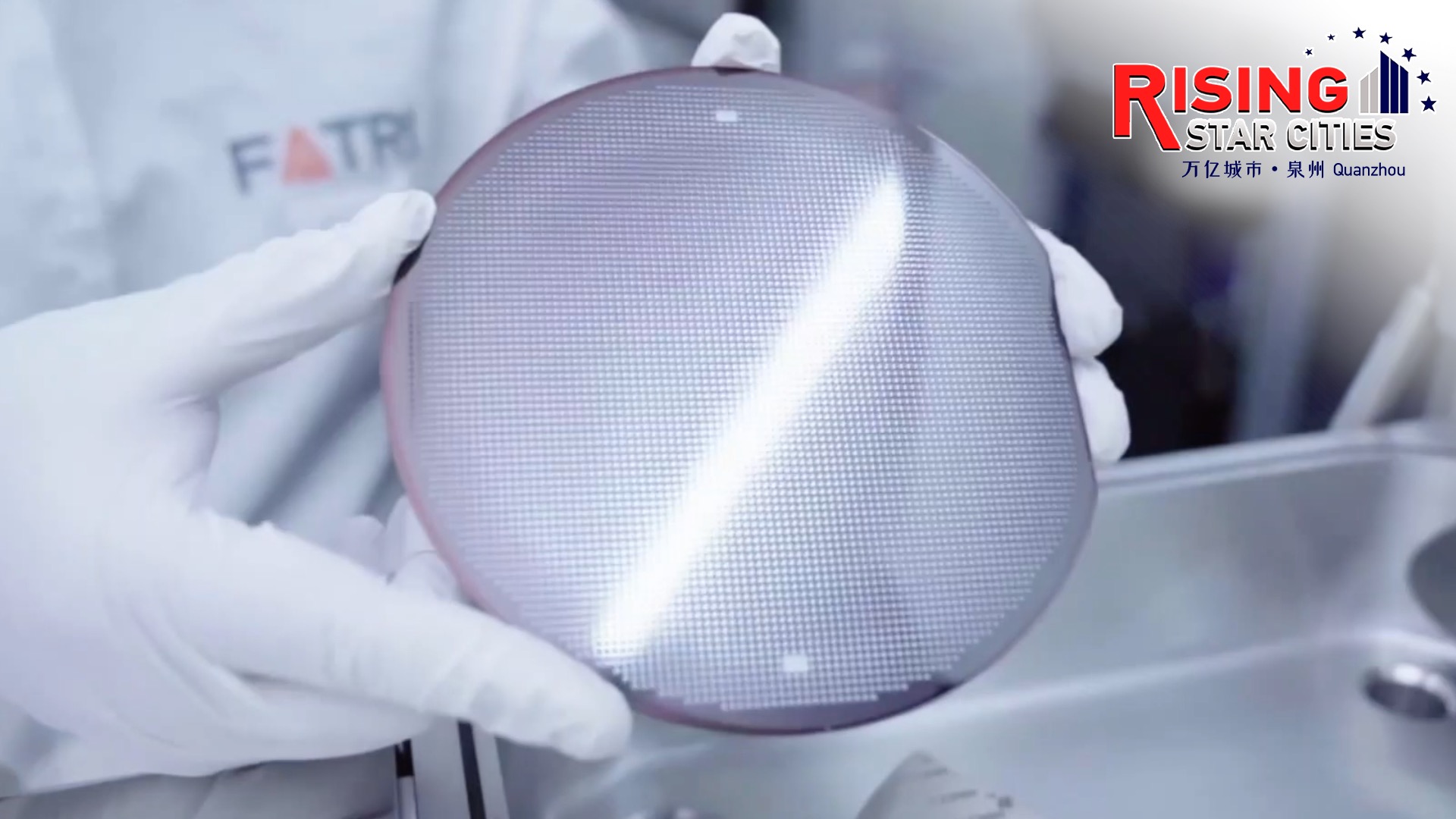
Han's Semiconductor has an insight into the market demand, and with years of accumulated technical advantages and industry experience, it launched the UV laser debonding solution as early as 2017, and successfully independently developed the first domestic laser debonding equipment.

Image


Comparison of various debonding technologies


In order to meet the needs of the rapid development of packaging technology, Han's Semiconductor continues to carry out technological innovation and iteration, and in 2020, it will launch the first domestic fully automatic laser debonding equipment DSI-S-DB661 that is compatible with separation and cleaning integration. Process verification of leading packaging customers in the industry, and successfully introduced into the production line to achieve large-scale application.

Fully automatic laser debonding equipment
DSI-S-DB661


1660923150241.png

1-Application field: It is used in fan-out wafer and panel-level advanced packaging such as consumer electronics processors and servers; 2.5D/3D stacking integration of ultra-thin devices such as memory chips Memory, Flash, and DRA; III-V and compound semiconductor RF chips, power devices, etc. Heterogeneous integration and thin-film processing.

2-Equipment advantage: 4, 6, 8, 12inch wafer or frame form a full range of responses;● Self-developed beam shaping system, spot uniformity >90%;● Real-time monitoring and feedback of laser power and energy;● Real-time tracking and feedback of laser focus;● Real-time monitoring and feedback of automatic separation tension;● Chemical wet cleaning and degumming;● Adapt to AGV and OHT automation operations;● SECS-GEM standard interface.

3-Device parameters

1660923199811.png


In the future, with the development of semiconductor technology and the emergence of new applications, there will be more application requirements for packaging technology. Han's Semiconductor has been fully prepared to continue to focus on the post-Moore era, give full play to the company's innovative technology advantages, and promote the breakthrough development of the integrated circuit industry with advanced technology.
 

ansy1968

Brigadier
Registered Member
He is warning his compatriot, come, join me and have a greener pasture here on the other side of the strait, a bonus we have a lot of @Loveleenkr look alike which you all adore and dream of dating...lol

Please, Log in or Register to view URLs content!

Please, Log in or Register to view URLs content!


11 hours ago — Tech war: Taiwanese veteran who helped China's memory chip progress says US-led Chip 4 Alliance could backfire on member countries -report ...
 

BoeingEngineer

Junior Member
Registered Member
Well, I think the issue is that domestic suppliers haven't fully ramped up yet, so they will still need to buy Western technology. If American suppliers can't provide after sale support, then every fab in China will want to move away from American suppliers as soon as possible.

What a disastrous and ridiculous policy by this stupid administration. It's like they are trying to kill successful American companies.

This Biden administration is the best thing ever happed to China !!

It will make China 100% tech independent from the West and become a true Hyper Power !!
 

BoeingEngineer

Junior Member
Registered Member
Honestly I am a bit dubious about this rumor.

I for sure believe that US administration is well capable of doing anything, even the most disruptive actions. But this seems to me a really absurd and desperate move.

I mean, the only company in China that has FinFet technology in production is SMIC. So to target FinFet it means to target SMIC. At this point just do it directly. US could invent some official excuse out of thin air and totally ban SMIC, like they did for Huawei.

But to forbid post-sales assistance and mainteinance on US tools already installed and in production, it really means to completely destroy what remains of US companies credibility. Not only for today, but for the future too.

On the China side the only affected firm would be SMIC and only for 14nm and 7nm nodes, on US side instead AMAT, LAM Research and KLA can say goodbye to Chinese market....maybe this is the real target of US administration.

Remember Lam, AMAT, KLA are not that important. They are nothing compare to ASML's EUV !!

China can easily within 1 year replace all LAM, AMAT and KLA with domestic companies.

This will completely destroy American semiconductors in the long run !!
 

hullopilllw

Junior Member
Registered Member
Remember Lam, AMAT, KLA are not that important. They are nothing compare to ASML's EUV !!

China can easily within 1 year replace all LAM, AMAT and KLA with domestic companies.

This will completely destroy American semiconductors in the long run !!
Better off be quiet than to give such bombastic statement. Chest thumping is of no use here.
 

ansy1968

Brigadier
Registered Member
We are all tired of America bullying entire world, in this way or another...
Bro Don't worry from the horse mouth itself CGTN, China complained is SOP since they're specially mention regarding the Chip Bill BUT deep inside there is smugness as in telling the Americans "Go Ahead Punk, Make My Day"...lol

China's IDM enterprises confident of achieving chip self-sufficiency
By Zhao Chenchen, Zhao Yuxiang

4cc37f2a161647beb5d70ec03e929a83.jpg

Editor's note: This report focuses on Quanzhou as part of our special series, "Rising Star Cities," about Chinese cities whose annual GDP exceeds 1 trillion yuan ($155 billion). At the end of 2021, there were 24 such cities. Click
Please, Log in or Register to view URLs content!
for more stories on Quanzhou, an ancient trading hub known for its cultural diversity. You can also explore our earlier coverage of
Please, Log in or Register to view URLs content!
,
Please, Log in or Register to view URLs content!
and
Please, Log in or Register to view URLs content!
.
With the recent $280 billion U.S. CHIPS and Science Act signed off by President Joe Biden, the competition between the U.S., China, the European Union, and other East Asian countries to shore up their semiconductor capabilities has become increasingly fierce. After a global chip shortage and amid a scarred post-pandemic economy, the shortages are now spreading from autos to smartphones and displays, elevating semiconductors onto the agendas of governments from Washington to Brussels and Beijing.
The big chip race
Apart from the United States, which allocates $52 billion in funding from the act for its own semiconductor manufacturing, other major economies have also rolled out packages to boost domestic semiconductor production and research.
The European Union outlined a €43-billion ($49 billion) bundle from public and private funding for the sector in February and the Japanese government has approved investment totaling 774 billion yen ($6.8 billion) for its domestic chip industry. South Korea aims to attract roughly $450 billion in private investment to build the world's biggest chipmaking base over the next decade.
"I think that this is a war for our chip industry," said Nie Yongzhong, CEO of semiconductor company FATRI Group based in Quanzhou, southeast China's Fujian Province.
FATRI, or Future Advanced Technology Research Institute, is an integrated device manufacturer (IDM) for sensor chips with comprehensive capabilities from chip design to manufacturing, packaging, and testing.
Where will China stand?
For now, most chip manufacturers that qualify as IDMs are in the U.S., the EU, and East Asia, but Nie believes that China needs and has the potential to incubate more of them.
"I think our current shortage exists because we need more IDM (enterprises)," he said.
EDA is a software analysis tool crucial used by chip designers across the entire semiconductor chip chain.
On August 12, the U.S. Bureau of Industry and Security announced a new ban on exporting EDA software for making 3nm and more advanced chips to China. The banned EDA software for gate-all-around field effect transistor (GAAFET) is the next-generation semiconductor tech that can help chips achieve a higher frequency and lower power consumption.
It is a highly advanced technology that has only been adopted by Samsung so far, while Intel and Taiwan Semiconductor Manufacturing Company (TSMC) are planning to use it.
An analyst told Chinese business news outlet Caixin that the ban will have a limited effect on China in the short term but will restrain China's development in advanced chip-making.
Foreign firms took 77 percent of the EDA market in China in 2020, according to China's CCID Consulting. However, local EDA providers like Primarius Technologies claimed they had "formed core key tools that can support advanced process nodes such as 7nm, 5nm, and 3nm," according to its company website.
However, Nie thinks the ban would further boost China's capability to achieve chip self-sufficiency as "IDMs can build their own integrated circuit (IC) databases, which will also boost the development of EDA companies."
Nie believes that the advancement of IDMs would also foster the growth of chip design talent, who would, by that time, contribute in building China's own fabrication facilities (fab), or outsourced production companies, with core intellectual property rights.
 
Status
Not open for further replies.
Top