I understand posting it once from one article or two times by accident, but this is like the fourth time I see this article posted here and don't even say nothing new, is just the same script read by different authors.Turns out China punishes financial malfeasance, unlike in the US.
You are using an out of date browser. It may not display this or other websites correctly.
You should upgrade or use an alternative browser.
You should upgrade or use an alternative browser.
Chinese semiconductor industry
- Thread starter Hendrik_2000
- Start date
- Status
- Not open for further replies.
Personally I would love for this thread to be more focused on technical stuff rather than political stuff.I understand posting it once from one article or two times by accident, but this is like the fourth time I see this article posted here and don't even say nothing new, is just the same script read by different authors.
can't we block these FT , BB and The Diplomat useless articles. ?Personally I would love for this thread to be more focused on technical stuff rather than political stuff.
enough is enough
On the contraire bro neither I'm a proud WAR (Wife Always Right) member, the problem is @Loveleenkr is just so adorable...lolThks. I will drink to that too.
By the way, I am not sure whether you are being sexist or doing it deliberately to drive Loveleenkr out of SDF for using our material without given credit.
can't we block these FT , BB and The Diplomat useless articles. ?
enough is enough
I don't care about the political stuff as long is not repeated again and again and again and is about Chinese semiconductors. Posting it once is more than enough, if someone is not sure is something is already posted or if the post is redundant, just go back a few pages to check.Personally I would love for this thread to be more focused on technical stuff rather than political stuff.
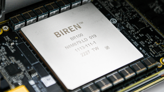
Specs of Biren GPU from Tom's Hardware
Chinese GPU developer introduces a 77 billion transistors chip.

(Image credit: Biren Technology)
has formally its first GPUs designed primarily for artificial intelligence (AI) and high-performance computing (HPC). According to the company, the top-of-the-range BR100 GPU can challenge Nvidia's A100 and even H100 chips in certain workloads, yet its complexity is comparable with that of Nvidia's .
Biren's initial family of compute GPUs includes two chips. The BR100 promises up to 256 FP32 TFLOPS or 2 INT8 PetaFLOPS performance, whereas the BR104 is rated for up to 128 FP32 TFLOPS or 1 INT8 PetaFLOPS performance.
The top-of-the-range comes with 64GB of HBM2E memory with a 4096-bit interface (1.64 TB/s), while the midrange with 32GB of HBM2E memory with a 2048-bit interface (819 GB/s).
Both chips support the INT8, FP16, BF16, FP32, and TF32+ data formats, so we're not talking about supercomputing formats (e.g., FP64) even though Biren says that its TF32+ format provides higher data precision than traditional TF32. Meanwhile, the BR100 and BR104 offer rather formidable peak performance numbers. In fact, if the company had incorporated GPU-specific functionality (texture units, render back ends, etc.) into its compute GPUs and had designed proper drivers, these chips would have been rather incredible GPUs (at least BR104, which is presumably a single-chip configuration).
In addition to the compute capabilities, Biren's GPUs can also support H.264 video encoding and decoding.
Biren's BR100 will be available in an OAM form-factor and consume up to 550W of power. The chip supports the company's proprietary 8-way BLink technology that allows the installation of up to eight BR100 GPUs per system. In contrast, the 300W BR104 will ship in a FHFL dual-wide PCIe card form-factor and support up to 3-way multi-GPU configuration. Both chips use a PCIe 5.0 x16 interface with the CXL protocol for accelerators on top, reports (via ).
Biren says that both of its chips are made using TSMC's 7nm-class fabrication process (without elaborating whether it uses N7, N7+, or N7P). The larger BR100 packs 77 billion transistors, outweighing the 54.2 billion with the Nvidia A100 that's also made using one of TSMC's N7 nodes. The company also says that to overcome limitations imposed by TSMC's reticle size, it had to use chiplet design and the foundry's CoWoS 2.5D technology, which is completely logical as Nvidia's A100 was approaching the size of a reticle and the BR100 is supposed to be even larger given its higher transistor count.
Given the specs, we can speculate that BR100 basically uses two BR104s, though the developer has not formally confirmed that.
To commercialize its BR100 OAM accelerator, Biren worked with Inspur on an 8-way AI server that will be sampling starting Q4 2022. Baidu and China Mobile will be among the first customers to use Biren's compute GPUs.
Chinese Biren's New GPUs Have 77 Billion Transistors, 2 PFLOPS of AI Performance
By published 1 day agoChinese GPU developer introduces a 77 billion transistors chip.

(Image credit: Biren Technology)
has formally its first GPUs designed primarily for artificial intelligence (AI) and high-performance computing (HPC). According to the company, the top-of-the-range BR100 GPU can challenge Nvidia's A100 and even H100 chips in certain workloads, yet its complexity is comparable with that of Nvidia's .
Biren's initial family of compute GPUs includes two chips. The BR100 promises up to 256 FP32 TFLOPS or 2 INT8 PetaFLOPS performance, whereas the BR104 is rated for up to 128 FP32 TFLOPS or 1 INT8 PetaFLOPS performance.
The top-of-the-range comes with 64GB of HBM2E memory with a 4096-bit interface (1.64 TB/s), while the midrange with 32GB of HBM2E memory with a 2048-bit interface (819 GB/s).
| Biren BR104 | Biren BR100 | Nvidia A100 | Nvidia H100 | |
| Form-Factor | FHFL Card | OAM Module | SXM4 | SXM5 |
| Transistor Count | ? | 77 billion | 54.2 billion | 80 billion |
| Node | N7 | N7 | N7 | 4N |
| Power | 300W | 550W | 400W | 700W |
| FP32 TFLOPS | 128 | 256 | 19.5 | 60 |
| TF32+ TFLOPS | 256 | 512 | ? | ? |
| TF32 TFLOPS | ? | ? | 156/312* | 500/1000* |
| FP16 TFLOPS | ? | ? | 78 | 120 |
| FP16 TFLOPS Tensor | ? | ? | 312/624* | 1000/2000* |
| BF16 TFLOPS | 512 | 1024 | 39 | 120 |
| BF16 TFLOPS Tensor | ? | ? | 312/624* | 1000/2000* |
| INT8 | 1024 | 2048 | ? | ? |
| INT8 TFLOPS Tensor | ? | ? | 624/1248* | 2000/4000* |
Both chips support the INT8, FP16, BF16, FP32, and TF32+ data formats, so we're not talking about supercomputing formats (e.g., FP64) even though Biren says that its TF32+ format provides higher data precision than traditional TF32. Meanwhile, the BR100 and BR104 offer rather formidable peak performance numbers. In fact, if the company had incorporated GPU-specific functionality (texture units, render back ends, etc.) into its compute GPUs and had designed proper drivers, these chips would have been rather incredible GPUs (at least BR104, which is presumably a single-chip configuration).
In addition to the compute capabilities, Biren's GPUs can also support H.264 video encoding and decoding.
Biren's BR100 will be available in an OAM form-factor and consume up to 550W of power. The chip supports the company's proprietary 8-way BLink technology that allows the installation of up to eight BR100 GPUs per system. In contrast, the 300W BR104 will ship in a FHFL dual-wide PCIe card form-factor and support up to 3-way multi-GPU configuration. Both chips use a PCIe 5.0 x16 interface with the CXL protocol for accelerators on top, reports (via ).
Biren says that both of its chips are made using TSMC's 7nm-class fabrication process (without elaborating whether it uses N7, N7+, or N7P). The larger BR100 packs 77 billion transistors, outweighing the 54.2 billion with the Nvidia A100 that's also made using one of TSMC's N7 nodes. The company also says that to overcome limitations imposed by TSMC's reticle size, it had to use chiplet design and the foundry's CoWoS 2.5D technology, which is completely logical as Nvidia's A100 was approaching the size of a reticle and the BR100 is supposed to be even larger given its higher transistor count.
Given the specs, we can speculate that BR100 basically uses two BR104s, though the developer has not formally confirmed that.
To commercialize its BR100 OAM accelerator, Biren worked with Inspur on an 8-way AI server that will be sampling starting Q4 2022. Baidu and China Mobile will be among the first customers to use Biren's compute GPUs.
CETC ion implanters used in the research of next gen wide band gap semiconducting sensing devices.
Generation of Spin Defects by Ion Implantation in Hexagonal Boron Nitride
Optically addressable spin defects in wide-band-gap semiconductors as promising systems for quantum information and sensing applications have recently attracted increased attention. Spin defects in two-dimensional materials are expected to show superiority in quantum sensing due to their atomic thickness. Here, we demonstrate that an ensemble of negatively charged boron vacancies (VB–) with good spin properties in hexagonal boron nitride (hBN) can be generated by ion implantation. We carry out optically detected magnetic resonance measurements at room temperature to characterize the spin properties of ensembles of VB– defects, showing a zero-field splitting frequency of ∼3.47 GHz. We compare the photoluminescence intensity and spin properties of VB– defects generated using different implantation parameters, such as fluence, energy, and ion species. With the use of the proper parameters, we can successfully create VB– defects with a high probability. Our results provide a simple and practicable method to create spin defects in hBN, which is of great significance for realizing integrated hBN-based devices.
Yeah I mentioned this before that some here (appix) posts same articles in multiple threads.I understand posting it once from one article or two times by accident, but this is like the fourth time I see this article posted here and don't even say nothing new, is just the same script read by different authors.
broadsword
Brigadier
Specs of Biren GPU from Tom's Hardware
Chinese Biren's New GPUs Have 77 Billion Transistors, 2 PFLOPS of AI Performance
By published 1 day ago
Chinese GPU developer introduces a 77 billion transistors chip.
Unfortunately, the brain is fabbed by TSMC.
- Status
- Not open for further replies.
