Chinese semiconductor industry

Status
Not open for further replies.

hvpc

Junior Member
Registered Member
450 mm wafers with immersion DUV would be an interesting strategy. This would require further development of domestic etch and deposition equipment with bigger chambers, superior temperature control, larger precision parts like quartz, ceramic, stainless, etc. It would require 100% fully automated fabs unlike manual 200 mm and semi-automatic 300 mm fabs. This takes advantage of Chinese advances in robotics and 5G communications to relay large amounts of data. But it does not require the development of entirely new equipment like EUV lithography which is an advantage.

Some challenges for IDMs: many analog fabs stick with 200 mm because the equipment is mostly used, for cost, but there's also a technical reason: they have large product variety in mid sized volumes so they need the flexibility of a more manual, lower volume, higher customizability 200 mm line. They need 1 type of product to justify 450 mm wafer adoption (i.e. multichip DPUs)

Some challenges for foundries: they need a stable customer base that wants to use 450 mm wafers. To prevent wasted capability and overproduction there needs to be a consistent high volume customer or alternatively, an advance in multiproject wafers that allows for 2 different types of chips to be put on 1 wafer. That means advances in mask making and in ready IP blocks so multiple customers can use the same IP block on their products i.e. a ready made SRAM subsection or serial communications subsection.
Making domestic 450mm immersion is not practical at all. You can’t have the cake and eat it, too. It’s already difficult to make a 300mm immersion, you can’t go expect a 450mm immersion scanner and expect it to be ready by 2025.
For example, UPrecisuon, as of late last year was still unable to make a competitive immersion dual stage for 300mm wafers. Asking them to come up with a stage that could handle 450mm stage while maintaining the scan speed would be even less attainable.
 

AndrewS

Brigadier
Registered Member
Making domestic 450mm immersion is not practical at all. You can’t have the cake and eat it, too. It’s already difficult to make a 300mm immersion, you can’t go expect a 450mm immersion scanner and expect it to be ready by 2025.
For example, UPrecisuon, as of late last year was still unable to make a competitive immersion dual stage for 300mm wafers. Asking them to come up with a stage that could handle 450mm stage while maintaining the scan speed would be even less attainable.

It's not just the immersion scanners.
I suspect that every piece of equipment in a fab would have to be redesigned to handle a 450mm wafer because it is significantly bigger than 300mm
 

hvpc

Junior Member
Registered Member
It's not just the immersion scanners.
I suspect that every piece of equipment in a fab would have to be redesigned to handle a 450mm wafer because it is significantly bigger than 300mm
Yes, of course. The entire supply chain needs to invest in the change

the industry as a whole abandoned the 450mm endeavor for a reason…the ROI just doesn’t make sense. The sheer amount of investment needed was just way too big to gain so little cost saving.

China is definitely welcome to go at it alone. But that would be insane. It was estimated it would take $30 or $40B for 450mm wafers (back in 2013 or 2014). I rather throw that money at SMEE, AMEC, UPrecision to give them more resources to speed up their pace of development.

UPrecision had to file for IPO last year to get more funding. They were still stuck at “developing the DWSi stage at 150wph” when ASML already reaching 300wph. So, I say, give these guy more money so they can focus on R&D and not worry about $.
 

tokenanalyst

Brigadier
Registered Member

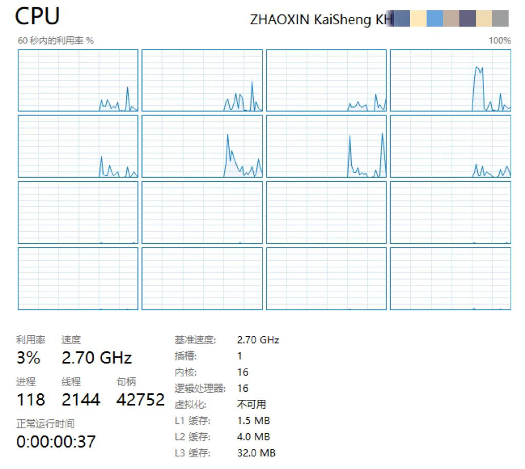
Suspected Zhaoxin new generation processor KH-40000 running score exposure​


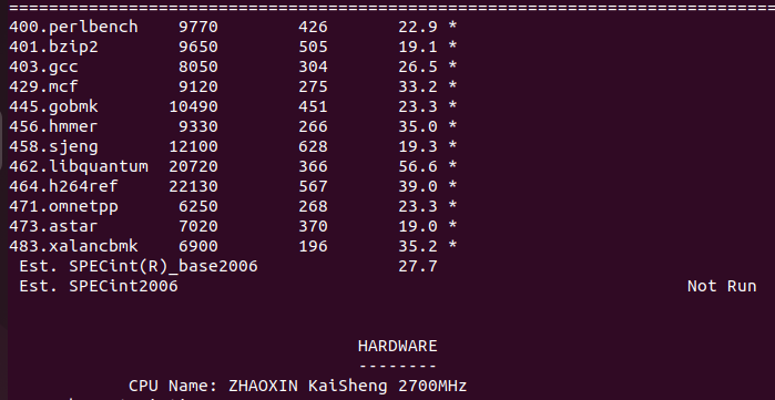
Recently, the SPEC CPU 2006 integer benchmark test scores of Zhaoxin's new-generation architecture processor KH-40000 appeared on Baidu Post Bar. The results show that the performance of Zhaoxin's new architecture has improved greatly, as shown below:

16558737469978.png


注 Ubuntu 22.04, gcc11.2 CINT_base

The exposed Zhaoxin processor operates at a frequency of 2.7G. According to Zhaoxin's official introduction, the KH-40000 adopts the new Yongfeng architecture, which is about 60% higher than the previous generation Wudaokou architecture IPC. The currently exposed SPEC CPU 2006 integer performance score is about 28 points, reaching the leading level of the independent architecture of domestic processors.

16558737579125.png


Note: Zhaoxin's new generation processor task manager information leak

It is reported that the KH-40000 series processors will be launched around August this year. There are workstation and server versions. The number of cores ranges from 8 to 32 cores, and the operating frequency is 2~2.8GHz.


Please, Log in or Register to view URLs content!

近日,百度贴吧上出现了兆芯新一代架构处理器KH-40000的SPECCPU2006整数基准测试跑分,结果显示兆芯新架构性能提升巨大。
 

daifo

Captain
Registered Member

Suspected Zhaoxin new generation processor KH-40000 running score exposure​


Recently, the SPEC CPU 2006 integer benchmark test scores of Zhaoxin's new-generation architecture processor KH-40000 appeared on Baidu Post Bar. The results show that the performance of Zhaoxin's new architecture has improved greatly, as shown below:

16558737469978.png


注 Ubuntu 22.04, gcc11.2 CINT_base

The exposed Zhaoxin processor operates at a frequency of 2.7G. According to Zhaoxin's official introduction, the KH-40000 adopts the new Yongfeng architecture, which is about 60% higher than the previous generation Wudaokou architecture IPC. The currently exposed SPEC CPU 2006 integer performance score is about 28 points, reaching the leading level of the independent architecture of domestic processors.

16558737579125.png


Note: Zhaoxin's new generation processor task manager information leak

It is reported that the KH-40000 series processors will be launched around August this year. There are workstation and server versions. The number of cores ranges from 8 to 32 cores, and the operating frequency is 2~2.8GHz.


Please, Log in or Register to view URLs content!

近日,百度贴吧上出现了兆芯新一代架构处理器KH-40000的SPECCPU2006整数基准测试跑分,结果显示兆芯新架构性能提升巨大。

Supposedly 16nm and comparable to the AMD EPYC 7601.

Please, Log in or Register to view URLs content!
 

gelgoog

Brigadier
Registered Member
Comparable my foot. It might have had a similar score as the AMD EPYC if it had a similar clock but it clocks much lower.

Look at this.
1655923521221.png
16nm processor was supposed to be KX-6000 and supposed to hit 3.0 GHz. Not 2.7 GHz.
If it is true that this indeed has 16 cores then maybe the 8 core will clock higher. But we will see.

The lower clock than Zen points to some kind of design issue which might not be solvable without a chip redesign.
And Zen core has already had Zen+, Zen 2, Zen 3 iterations since that.
I mean it is not a bad effort assuming it doesn't have any bugs. But let us be realistic here.

16nm also points to it being fabbed at TSMC in China. I had heard rumors the delays were due to change to SMIC 14nm or even 10nm process. But looking at this leak it seems the delays were they couldn't get the thermals down and get it to clock properly. I hope next time they will make a chip for SMIC or HLMC 14nm or better and get someone from Phytium or HiSilicon to fix the clockspeed issues in the architecture.

If they want to go for high core counts then they also need to consider using chiplets like AMD is doing.
 
Last edited:

european_guy

Junior Member
Registered Member
Comparable my foot. It might have had a similar score as the AMD EPYC if it had a similar clock but it clocks much lower.

AMD EPYC 7601 was a 14nm design released in mid 2017 and clocked at 2.2GHZ with max single core boost at 3.2 GHZ, so more or less should be compatible also by design rules (16nm vs 14nm).

If the August release will be confirmed, it is a 5 years gap, that is not a lot considering that design and fabrication is 100% Chinese and that PC processor evolution nowadays is very slow, almost stagnant, mainly PC are already good enough for 95% of their typical uses. Indeed an important milestone.

Please, Log in or Register to view URLs content!
 

gelgoog

Brigadier
Registered Member
AMD EPYC (Naples) had versions up to 32 cores. Not 16.
It also had SMT. So 64 threads. Does this processor have SMT? The older ones did not.
The SMT will make a major difference in things like web servers.

Sure, it is a major achievement, and now Hygon's licensed processors probably aren't necessary anymore. I am also typing this on a processor from 14nm era. I doubt I will buy a new processor until Zen 4 or later. I think the big milestones will be 5nm, first major EUV node, and then 2nm because of the new transistors. But why TSMC?
 

ansy1968

Brigadier
Registered Member
TSMC had been bamboozled by the US, you're not white enough, you too Samsung, Eric Schmidt had wrote an opinion piece and is damming, the conclusion Intel is the favored son and you two are a bastard son, so the two of you will not get a snippet of wealth from me...lol

Currently, both TSMC and
Please, Log in or Register to view URLs content!
in the U.S., but in Schmidt and Allison’s view, the U.S. needs to do more to ensure America’s long-term prosperity.

Previously, the U.S. government proposed a $52 billion chip support plan, which is still under review by U.S. lawmakers. Beyond that, the ex-Google CEO and Allison argue the U.S. should leverage its R&D advantage by making less advanced but more widely used slower chips through the likes of Intel and GlobalFoundries. It should also redouble efforts to get
Please, Log in or Register to view URLs content!
and Samsung builds a factory in the United States.


Please, Log in or Register to view URLs content!


2 days ago — The ex-Google CEO believes that the United States should encourage chip foundry giants to cooperate with American chip design companies.
 

gelgoog

Brigadier
Registered Member
Those comments in the article are pure comedy gold. But all of them miss the point.
These people never heard of Moore's Second Law.
Please, Log in or Register to view URLs content!

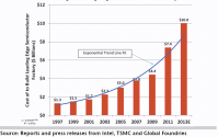
i.e. "the cost of a semiconductor chip fabrication plant doubles every four years"

See the thing about the US granting 57 billion USD to build fabs? And that not even matching what TSMC can spend?
Now consider the economic "law" above. Why do you think integrated manufacturers like Intel keep vanishing and foundries like TSMC are now the standard? Why do you think several companies have to share a fab? Why does the amount of companies at the leading edge keep shrinking? Why do we need to keep increasing wafer size? It is to keep cost per transistor low enough.

This means whoever has the market and the volume to keep those factories fed will win. Keep them at low utilization rate and you lose money, billions, on each fab. And the US market long since stopped being large enough to justify the latest generation of fabs. At one point Japan's market was large enough too but then it wasn't. China's is still large enough.

1655947386690.png
 
Last edited:
Status
Not open for further replies.
Top