Chinese semiconductor industry

Status
Not open for further replies.

tphuang

Lieutenant General
Staff member
Super Moderator
VIP Professional
Registered Member
A chip company raised 2 billion yuan in 15 months.

Tianshu Zhixin launched the general-purpose GPU design in 2018, and its "Tiangai 100" achieved mass production last year, with product orders exceeding 230 million yuan.
The money raised is not the impressive part here, but rather that they already got orders for 230 million RMB. I posted this a few weeks ago when they announced that number. It was quite impressive considering they've just started mass producing chips. Keep in mind that is a larger number in order revenue than what Kunlun-2 has achieved thus far. That shows the massive market in China looking to get off American product. 230 million -> $30 to 35 million. My guess that's around 20000 chips or more ordered. That's pretty good for a new product.

The one thing that really annoyed me about Tianshu is that they said Nvidia has 95% of the market and Chinese chipmakers fight for the remaining 5%. That is real defeatist attitude.

This is the kind of stuff that really helps them. Inspur will help putting great performance into these new Chinese chips. All these new domestic chipmakers work with Inspur to put their product in actin.
Please, Log in or Register to view URLs content!

Please, Log in or Register to view URLs content!
took only 1 year for them to start mass producing Tiangai 100. From when mass production start in December of 2021 until August, they have now served over 200 types of AI training. Uses 7 nm technology like most other Chinese AI chips. Hint hint, SMIC N+2 will handle this eventually.

They have also shown Zhikai-100 (智铠100) recently and that will start mass production at end of this year. It's already getting tested with first set of clients. So definitely keep an eye on them.

But there are so many new guys now and we will have to wait a while to see who "wins"

A sign of things to come, Apple refuse to accept TSMC price hike. TSMC bargaining power is slowing ebbing, can't ask customer to pay extra premium especially IF its your only sole client for the 3nm technology, They are now regretting ditching Huawei....lol

The Mainland Chinese tech company had been reading this, the reason why they won't invest a battery factory in the US to service Apple, exclusivity is a double edge sword, your company may grow exponentially BUT you are at their mercy and whims.

And I'm thinking the much hype Apple Car is vaporware, expected to be release in 2025, by that time its Chinese Rivals had taken over the market. Hoping to seizes the premium segment with the downturn and incoming depression, good luck with that and lets see IF it hit the ground running. ;)

With demand cascading and massive increase in FAB capacity, who among the major FABS will thrive?
Ideally for China, this downturn will force TSMC and Apple to stop pushing as hard for next generation chips. At the same time, SMIC needs to speed up its advanced node production. I know that it's probably more profitable for them to keep building fabs for 28 nm and higher nodes. However, Chinese gov't needs to step in and tell SMIC to focus on expanding its advanced node production.

There are so many Chinese chipmakers who are in trouble if TSMC gets cut off from them. The sooner they get shifted to SMIC's N+1/N+2 process, the sooner TSMC will really feel the pain. Long term, TSMC's biggest competition is China, not Samsung.

When TSMC and MediaTek start to lose orders to mainland firms, they will need to start cutting staff. When that happens, I would bet most of them would rather move to Shanghai than Arizona. The thing that American semiconductor industry complains about is not having enough people going into this industry. That's why they want to bring in Taiwanese workers. Based on personal experience, Taiwanese are not like HKers. Aside from the ones with Western roots, they rest of them move to mainland or HK for better opportunity in life. And if you can continue to weaken TSMC/MediaTek, most of the people that leave will come to mainland to work!

That's how you win in this. It's the people behind these companies that drive them forward. You need to get the best people. The way to do that is continually making the mainland firms more appealing to them and making Taiwanese firms weaker.
 

ansy1968

Brigadier
Registered Member
Ideally for China, this downturn will force TSMC and Apple to stop pushing as hard for next generation chips. At the same time, SMIC needs to speed up its advanced node production. I know that it's probably more profitable for them to keep building fabs for 28 nm and higher nodes. However, Chinese gov't needs to step in and tell SMIC to focus on expanding its advanced node production.
Sir from the discussion between @FairAndUnbiased and @Jianguo about both CFET and nVSAFET which were developed in China with almost no foreign participation. I believed the table provided by @Alb is a distinct possibility. With SN1 and SN2 FABS leading the way for advance node production as both ASML and SMIC look for domestic substitute suppliers.
There are so many Chinese chipmakers who are in trouble if TSMC gets cut off from them. The sooner they get shifted to SMIC's N+1/N+2 process, the sooner TSMC will really feel the pain. Long term, TSMC's biggest competition is China, not Samsung.

When TSMC and MediaTek start to lose orders to mainland firms, they will need to start cutting staff. When that happens, I would bet most of them would rather move to Shanghai than Arizona. The thing that American semiconductor industry complains about is not having enough people going into this industry. That's why they want to bring in Taiwanese workers. Based on personal experience, Taiwanese are not like HKers. Aside from the ones with Western roots, they rest of them move to mainland or HK for better opportunity in life. And if you can continue to weaken TSMC/MediaTek, most of the people that leave will come to mainland to work!

That's how you win in this. It's the people behind these companies that drive them forward. You need to get the best people. The way to do that is continually making the mainland firms more appealing to them and making Taiwanese firms weaker.
Sir among the major FABS maker the Chinese will be the least affected as the local demand is huge and it's a moving target with the demand for chips use in NEV is increasing. The strategy is to dominate the 28nm market with local substitute maybe the 70% criteria on Made in China 2025 is based on this node and we read it wrong. ;)
 

FairAndUnbiased

Brigadier
Registered Member

GaNo Opto launches first silicon carbide EUV photodiode​

GaNo Optoelectronics Inc – a spin-off from China’s Nanjing University that offers ultraviolet (UV) detectors and modules based on wide-bandgap semiconductors including gallium nitride (GaN) and silicon carbide (SiC) – has formally released what it claims are the first commercial SiC-based extreme ultraviolet (EUV) photodiodes.

Figure 1: Distribution of optical emission spectrum from THz to x-ray.


Figure 1: Distribution of optical emission spectrum from THz to x-ray.

With the rapid development of VLSI fabrication technologies down to 7/5nm nodes (for micro-chips containing billions of transistors), advanced photolithography is transitioning from deep ultraviolet (DUV) immersion lithography based on a 193nm light source to extreme ultraviolet (EUV) lithography based on 13.5nm light source. An EUV lithography system is so complex that demanding technical challenges must be overcome for meeting chipmakers’ requirements for high-volume manufacturing. Among them, the development of high-performance EUV detectors is critical because, to precisely control the photoresist exposure dose, the intensity and uniformity of the EUV light beam must be constantly monitored. Besides EUV lithography, semiconductor EUV detectors are also core components in solar-observing satellites, materials science and many fundamental research fields.

Traditionally, commercial EUV detectors are solely based on silicon (Si), which have been demonstrated with certain success but suffer from several intrinsic drawbacks. For example, although silicon EUV detectors could exhibit moderate quantum efficiency in the EUV wavelength range, they require highly complex optical filters to achieve a high UV/visible rejection ratio as their peak response stays within the visible wavelength range. In addition, silicon detectors are not suitable for working in harsh environments, which would degrade considerably upon high-fluence EUV irradiation.

“It has been well accepted that wide-bandgap semiconductor is the most suitable material for making UV photodetectors,” says chief technology officer Dr Hai Lu, who is also distinguished professor at Nanjing University. “Due to the wide-bandgap nature of SiC, EUV photodiodes based on SiC have no response to background white light and could exhibit very low dark current down to 1pA even at a high temperature of 150℃. This means that the SiC EUV photodiodes have extremely low noise, leading to very high signal-to-noise ratio and detectivity. Meanwhile, it has been confirmed that the radiation hardness of SiC photodiodes is at least 1000 times higher than their silicon counterparts, due to the high electron-hole pair ionization energy and displacement threshold energy of SiC semiconductor,” he adds.

GaNo Opto says that its new intrinsically visible-blind EUV photodiodes can work in either photovoltaic or photoconductive mode with high EUV photon detection efficiency, high response speed and high stability.

Despite the apparent advantages, the implementation of SiC EUV photodiodes is very challenging due to substrate- or epi-related material defects, relatively poorly modeled device operation, and immature device processing technology. “Our process shows that appropriate surface electric field modulation and surface passivation techniques are critical for realizing SiC EUV photodiodes with low leakage current and long-term stability, both of which are necessary for high-end applications in advanced lithography systems or space satellites,” Lu says.

Figure 2: Some of GaNo Opto’s newly released EUV and vacuum UV detectors.


Figure 2: Some of GaNo Opto’s newly released EUV and vacuum UV detectors.

After pilot production and multiple customer verifications beginning from October 2021, GaNo Opto has started to ship SiC EUV photodiodes and components to several major customers worldwide.

“Our next step is to develop EUV imaging arrays based on SiC photodiodes,” says Lu. “In this case, uniformity among each photodiode pixel and scalability would be the main technological barriers. New implantation and dopant activation sequences, and back-end processing techniques, are being developed to achieve this goal.”

Please, Log in or Register to view URLs content!
wonder how they'll disperse EUV wavelengths for EUV spectroscopy.
Please, Log in or Register to view URLs content!


if they do come out with an EUV spectrometer it will be an impressive achievement as few organizations are capable of that today.
 

tokenanalyst

Brigadier
Registered Member

Dinglong Co., Ltd.: At present, it has made a breakthrough in the aluminum process polishing liquid product of the 28nm node HKMG process​


Jiwei.com News Recently, Dinglong Co., Ltd. said in an institutional survey that the company's CMP polishing pad products have deeply penetrated into the supply chain of various domestic mainstream wafer fabs, becoming a supply for some customers, and the heavy volume of other customers has also changed. As planned, the company has an obvious leading advantage in import substitution in the domestic market, and the performance of CMP polishing pads in the first half of this year has also increased significantly.

In terms of the overall trend, due to the expansion of domestic downstream wafer fab production lines and the gradual increase in production, the progress of the process has brought about an increase in the number of CMP processes, which expands the demand for CMP core consumables, and the trend of integrated circuit supply chain autonomy is obvious. In the future, the domestic market space for CMP polishing pads will further increase, and the company, as the only domestic supplier of CMP polishing pads in China that fully masters the core R&D and manufacturing technology of the entire polishing pad process, will also gain more opportunities. At the same time, the company is also actively exploring overseas customers of CMP polishing pads, and the related market work is progressing as planned.

Different from the CMP polishing pad market, some types of CMP polishing liquids in China have been replaced by themselves. Therefore, in the process of early product development and customer communication, the company prioritized the domestic failure to achieve replacement, and downstream fab customers also The urgently needed imported CMP polishing solution has been deployed. At present, breakthroughs have been made in the aluminum process polishing solution of the 28nm node HKMG process and the oxide layer polishing solution equipped with self-produced high-purity silicon oxide abrasives. More than 20 polishing liquid products such as copper process, metal aluminum process, barrier layer process, metal tungsten process, and dielectric layer process are laid out across the board. On the whole, this is a differentiated strategy. At this stage, it can effectively avoid homogeneous competition among domestic material manufacturers, and it also reflects the company's innovative thinking and R&D capabilities.

Please, Log in or Register to view URLs content!
 

tokenanalyst

Brigadier
Registered Member

Nanda Optoelectronics: 7 precursor products are currently being supplied in large quantities to major customers including SMIC, YMTC, etc.​


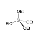
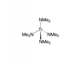
Recently, NTU Optoelectronics said in an institutional survey that the precursor business currently supplies 7 products such as TEOS (for silicon plasma ALD) and TDMAT (for titanium plasma ALD) in large quantities. The customers are mainly chip manufacturers, such as SMIC and YMTC.

With the dual support of its own R&D technology accumulation and outsourced patents, NTU’s R&D and industrialization layout in the field of advanced precursor materials has been well established. %. With the further advancement of industrialization and the continuous expansion of the market, the precursor business is expected to become the company's new business growth point.

Regarding the possibility of failure of the silicon precursor patent purchased by the company from DuPont in the United States under the situation of Sino-US trade tension, NTU said that when the company purchased the silicon precursor patent, the corresponding products were only available in the laboratory stage. The output is not sold on the market and is not included in the relevant restricted list.

The company purchased the ownership of the relevant patents, and the registration and filing procedures for changing the patentee have been completed. Therefore, the company has full autonomy over these silicon precursor patents.

The main energy of Ningbo Nanda Optoelectronics Co., Ltd., the main body of its photoresist project, is to focus on the customer certification of ArF photoresist, and strive to achieve large-scale sales and industrialization as soon as possible.

It said that the technology of ArF photoresist can be extended to the direction of KrF photoresist, and the follow-up company will determine whether to carry out the research and development and industrialization of KrF photoresist according to the progress of the project and the market situation. The supporting materials required for the production of ArF photoresist, such as important monomers, developing solutions, etc., are independently developed and produced by the company. For materials with domestic production capacity, the company adopts domestic procurement. The company has always insisted on fundamentally solving the "stuck neck" problem of ArF photoresist, and building a complete industrial chain from supporting materials to advanced photoresist products.

Please, Log in or Register to view URLs content!

1664419822841.png1664419859411.png
 

paiemon

Junior Member
Registered Member
Ideally for China, this downturn will force TSMC and Apple to stop pushing as hard for next generation chips. At the same time, SMIC needs to speed up its advanced node production. I know that it's probably more profitable for them to keep building fabs for 28 nm and higher nodes. However, Chinese gov't needs to step in and tell SMIC to focus on expanding its advanced node production.

If SMIC was buying the most advanced DUV systems from ASML, I would suspect that they are prepping for expanding advanced node production even if in the near term they may only be focused on more mature nodes due to a faster path forward due to more readily available equipment, etc. There may be other bottlenecks in building out advanced nodes besides just ASML, and if it is going to be year long or more delay to clear those it would make sense to just go with the readily available nodes and start earning the profits. It would seem wasteful to use a top of line DUV designed for advanced nodes solely on mature nodes when a cheaper system could do the same, so if maximizing profit at mature nodes was the true goal they would probably just order older systems since the buildout would be more cost-effective.
 

ansy1968

Brigadier
Registered Member
If SMIC was buying the most advanced DUV systems from ASML, I would suspect that they are prepping for expanding advanced node production even if in the near term they may only be focused on more mature nodes due to a faster path forward due to more readily available equipment, etc. There may be other bottlenecks in building out advanced nodes besides just ASML, and if it is going to be year long or more delay to clear those it would make sense to just go with the readily available nodes and start earning the profits. It would seem wasteful to use a top of line DUV designed for advanced nodes solely on mature nodes when a cheaper system could do the same, so if maximizing profit at mature nodes was the true goal they would probably just order older systems since the buildout would be more cost-effective.
Topline ASML are used in SN1 and SN2 FAB (100,000 wpm scalable to 150,000), expansion FAB in Beijing, Tianjin, Shenzhen, Shanghai Lingang and Chongqing will be using mix with majority domestic DUVL with IOC next year with full operation in 2024. Can SMEE deliver? with 4 months before 2023, yes it can! ;)
 

paiemon

Junior Member
Registered Member
Topline ASML are used in SN1 and SN2 FAB (100,000 wpm scalable to 150,000), expansion FAB in Beijing, Tianjin, Shenzhen, Shanghai Lingang and Chongqing will be using mix with majority domestic DUVL with IOC next year with full operation in 2024. Can SMEE deliver? with 4 months before 2023, yes it can! ;)
Thank you for clarifying, that would make alot of sense.
 

Quickie

Colonel
SMIC should use a black market middleman and offer to buy those idled EUVL machines anonymously in cash lol. Anyone with a brain will suspect it's SMIC or another Chinese company, but who will say no to a 9 digit offer in suitcases of hard cash?

Then would planes be suddenly gone missing with hundreds of passengers aboard? One of the conspiracy theories that came out in such a real-life event had to do with the transfer of advanced technology/chips to China.
 
Status
Not open for further replies.
Top