
You are using an out of date browser. It may not display this or other websites correctly.
You should upgrade or use an alternative browser.
You should upgrade or use an alternative browser.
Chinese semiconductor industry
- Thread starter Hendrik_2000
- Start date
- Status
- Not open for further replies.
KMT accuses government of not protecting TSMC
The Chinese Nationalist Party (KMT) caucus yesterday accused President Tsai Ing-wen (蔡英文) of caving in to the US’ demand that Taiwan Semiconductor Manufacturing Co (TSMC) hand over confidential information.
- By Lin Liang-sheng and Jonathan Chin / Staff reporter, with staff writer
The US Department of Commerce on Sept. 23 asked US and foreign semiconductor companies, including TSMC and South Korea’s Samsung Electronics Co, to provide information on chip inventory and sales within the next 45 days, media reports said.
US President Joe Biden’s administration is considering invoking the Defense Production Act to force companies to provide the information, the reports said.
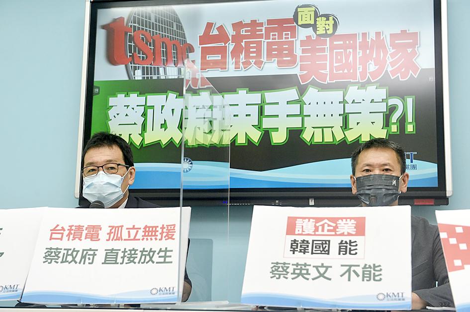
Chinese Nationalist Party (KMT) caucus whip Alex Fei, left, and KMT Legislator Lin Wei-chou hold a news conference at the Legislative Yuan in Taipei yesterday, accusing the government of not supporting Taiwan Semiconductor Manufacturing Co against US pressure.
Photo: George Tsorng, Taipei Times
US Secretary of Commerce Gina Raimondo was cited by Reuters as saying that the request for information on the chip crisis would strengthen supply chain transparency and that “other tools” would be brought to bear on companies that did not comply.
The Tsai administration and Minister of Economic Affairs Wang Mei-hua (王美花) are willing to sacrifice TSMC’s interests to comply with the US’ wishes, the KMT caucus told a news conference in Taipei.
Urging the Ministry of Foreign Affairs and the Ministry of Economic Affairs to lodge a protest with Washington, the caucus said it is prepared to bring its case to the Legislative Yuan.
The government should get tough with the US, as Washington’s actions contravene Article 2 of the Trade Secrets Act (營業秘密法), KMT Legislator William Tseng (曾銘宗) said.
“The government has to protect the Republic of China’s economic interests and those of TSMC’s 950,000 shareholders,” Tseng said.
Tsai should consider demanding that Intel also provide confidential information about its inventory if the US insists on demanding the same from TSMC, he said.
The US has repeatedly used the Sherman Antitrust Act and other legal mechanisms to force foreign industries to surrender trade secrets or technologies since the 1980s, KMT caucus whip Alex Fai (費鴻泰) said.
The use of such methods led to the downfall of Japanese companies Toshiba and Hitachi, he added.
Should TSMC give up confidential information about its manufacturing process, orders and inventory, it could lose its competitive edge, and its ability to act as the “sacred mountain guarding the nation,” he said.
Tsai is lying to the country about how Washington’s request would not hurt the chipmaker, Fai said, adding that the government would surely have rejected the request had it come from Beijing.
Tsai should not have prostrated the nation before the US or be indifferent to its unreasonable demands, he added.
“This shows that Tsai, Wang and the Democratic Progressive Party are cowards,” Fai said.
KMT Legislator Lin Wei-chou (林為洲) said that South Korea has reacted promptly by creating a committee with its semiconductor sector to put up a coordinated response to the US’ demands.
Taipei should follow Seoul’s example and not leave TSMC to fight Washington alone, Lin said
This would be particularly painful considering how much of taiwan's resources were poured into developing TSMC into what it is today, and it was done during the KMT's tenure as a a dictatorship under the Chiangs.
But i'm not surprised, the DPP have a hate boner against Chiang and the KMT so it'd make sense that they'd do everything they can to trash all mainlander/weishengren projects and monuments, including TSMC.
λ/12 Super Resolution Achieved in Maskless Optical Projection Nanolithography for Efficient Cross-Scale Patterning
Interesting research made by the Chinese Academy of Science on mask-less lithography, were they managed to create 32nm features with a 384nm light source.

Interesting research made by the Chinese Academy of Science on mask-less lithography, were they managed to create 32nm features with a 384nm light source.
Last edited:
Hendrik_2000
Lieutenant General
Via vincent Another advance in semi packaging eqpt
Source: Aijiwei
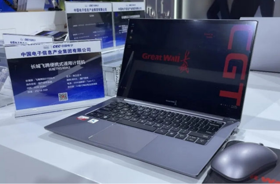
#the Great Wall#

8 days ago
According to the micronet news, on September 29, the Zhengzhou Rail Transit Information Technology Research Institute under the Great Wall of China and Henan General Intelligent Equipment Co., Ltd. completed the technical iteration of the semiconductor laser invisible wafer cutting equipment in just one year. The rate has been increased from 100nm to 50nm, reaching the highest precision in the industry, realizing the function of wafer backcutting. At the same time, continuous optimization of the process, based on the original technology of cutting silicon materials, has achieved technological breakthroughs in processing CIS, RFID, silicon carbide, gallium nitride and other materials, which has a milestone significance for further improving my country's smart equipment manufacturing capabilities. .
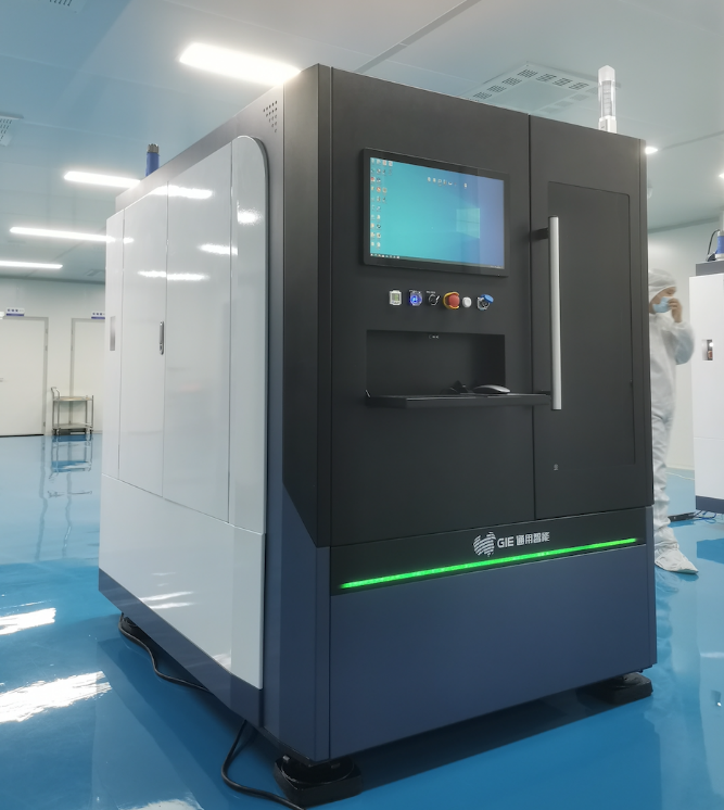
(HGL1341 Wafer Laser Hidden Cutting Equipment)
It is reported that the semiconductor industry is known as the pearl of the national industry, and wafer cutting is an indispensable key process in the semiconductor packaging and testing process and the "heart" of the semiconductor industry. Thousands, tens of thousands, or even 100,000 "independent functional dies" are gathered on each wafer after "circuit production". The quality of the wafer segmentation process directly determines the "production efficiency" and the "production efficiency" of the semiconductor process chain. The pros and cons of "competitiveness".
In May 2020, Zhengzhou Railway Transportation Institute under the Great Wall of China and Henan General Intelligent Equipment Co., Ltd. developed my country’s first semiconductor laser invisible wafer cutting machine, filling the domestic gap and breaking foreign countries in semiconductor laser invisible wafer cutting technology. Monopoly, key technical performance parameters have reached the world's leading level, opening the prelude to the development of my country's laser wafer cutting industry.
The resolution from 100nm to 50nm is an iterative upgrade. Liu Zhenyu, Vice President of China Great Wall and Dean of Zhengzhou Rail Transit Institute, introduced that the laser wafer stealth cutting equipment after iterative upgrade can freely control the depth of the laser focus point, the length of the focus point, and the freedom to control the distance between the two focus points. Through the use of special materials, special structure design, and special motion platform, it can maintain high stability and high precision cutting under the high-speed movement of 500mm/S. The laser focus is only 0.5um, and the cutting traces are more delicate. Avoid damage to the surface of the material, and greatly improve the quality, efficiency, and benefit of chip manufacturing.
According to reports, the equipment can be widely used in high-energy integrated circuit products, including CPU manufacturing, image processing ICs, automotive electronics, sensors, and the manufacturing of new-generation memories. It is significant for solving the "stuck neck" problem of high-end smart equipment in my country's semiconductor field. effect. (Proofreading/Arden)
Upgrade from 100nm to 50nm! China Great Wall Semiconductor's laser invisible wafer cutting technology has made a major breakthrough
Source: Aijiwei
#the Great Wall#
8 days ago
According to the micronet news, on September 29, the Zhengzhou Rail Transit Information Technology Research Institute under the Great Wall of China and Henan General Intelligent Equipment Co., Ltd. completed the technical iteration of the semiconductor laser invisible wafer cutting equipment in just one year. The rate has been increased from 100nm to 50nm, reaching the highest precision in the industry, realizing the function of wafer backcutting. At the same time, continuous optimization of the process, based on the original technology of cutting silicon materials, has achieved technological breakthroughs in processing CIS, RFID, silicon carbide, gallium nitride and other materials, which has a milestone significance for further improving my country's smart equipment manufacturing capabilities. .
(HGL1341 Wafer Laser Hidden Cutting Equipment)
It is reported that the semiconductor industry is known as the pearl of the national industry, and wafer cutting is an indispensable key process in the semiconductor packaging and testing process and the "heart" of the semiconductor industry. Thousands, tens of thousands, or even 100,000 "independent functional dies" are gathered on each wafer after "circuit production". The quality of the wafer segmentation process directly determines the "production efficiency" and the "production efficiency" of the semiconductor process chain. The pros and cons of "competitiveness".
In May 2020, Zhengzhou Railway Transportation Institute under the Great Wall of China and Henan General Intelligent Equipment Co., Ltd. developed my country’s first semiconductor laser invisible wafer cutting machine, filling the domestic gap and breaking foreign countries in semiconductor laser invisible wafer cutting technology. Monopoly, key technical performance parameters have reached the world's leading level, opening the prelude to the development of my country's laser wafer cutting industry.
The resolution from 100nm to 50nm is an iterative upgrade. Liu Zhenyu, Vice President of China Great Wall and Dean of Zhengzhou Rail Transit Institute, introduced that the laser wafer stealth cutting equipment after iterative upgrade can freely control the depth of the laser focus point, the length of the focus point, and the freedom to control the distance between the two focus points. Through the use of special materials, special structure design, and special motion platform, it can maintain high stability and high precision cutting under the high-speed movement of 500mm/S. The laser focus is only 0.5um, and the cutting traces are more delicate. Avoid damage to the surface of the material, and greatly improve the quality, efficiency, and benefit of chip manufacturing.
According to reports, the equipment can be widely used in high-energy integrated circuit products, including CPU manufacturing, image processing ICs, automotive electronics, sensors, and the manufacturing of new-generation memories. It is significant for solving the "stuck neck" problem of high-end smart equipment in my country's semiconductor field. effect. (Proofreading/Arden)
Tsinghua launches its first 12-inch ultra-precision wafer thinning machine
Versatile-GP300 is a 12-inch wafer thinning and polishing machine newly developed by the company for 3D IC manufacturing. It integrates ultra-precision grinding, CMP and post-cleaning processes through a new machine layout, and is equipped with advanced thickness deviation and surface defect control. Technology, provides a variety of system function expansion options, has the advantages of high precision, high rigidity, and flexible process development. It can expand and develop a variety of configurations based on Versatile-GP300 to meet the needs of wafer thinning technology in 3D IC manufacturing, advanced packaging and other fields.

Disaster always bring new opportunities and is only in hard times that you discover people's real talent.
Without Americans sanctions most Chinese equipment and software companies in their semiconductor industry would have been relegated to niche markets without an opportunity to grow. But now an American sanction asteroid has hit the heart of China electronic industry and from the smoke new opportunities has risen for those small companies and individuals researchers. The neocon hawks in the national security complex as always have ignore that they are smart hard working people.
Without Americans sanctions most Chinese equipment and software companies in their semiconductor industry would have been relegated to niche markets without an opportunity to grow. But now an American sanction asteroid has hit the heart of China electronic industry and from the smoke new opportunities has risen for those small companies and individuals researchers. The neocon hawks in the national security complex as always have ignore that they are smart hard working people.
Would they be stupid enough to turn on TSMC though? Didn't DPP claim that TSMC is the stabilizing force for Taiwan or something like that?This would be particularly painful considering how much of taiwan's resources were poured into developing TSMC into what it is today, and it was done during the KMT's tenure as a a dictatorship under the Chiangs.
But i'm not surprised, the DPP have a hate boner against Chiang and the KMT so it'd make sense that they'd do everything they can to trash all mainlander/weishengren projects and monuments, including TSMC.
Is this "Great Wall" company related to Great Wall Motors?Via vincent Another advance in semi packaging eqpt
Upgrade from 100nm to 50nm! China Great Wall Semiconductor's laser invisible wafer cutting technology has made a major breakthrough
Source: Aijiwei
#the Great Wall#
8 days ago
According to the micronet news, on September 29, the Zhengzhou Rail Transit Information Technology Research Institute under the Great Wall of China and Henan General Intelligent Equipment Co., Ltd. completed the technical iteration of the semiconductor laser invisible wafer cutting equipment in just one year. The rate has been increased from 100nm to 50nm, reaching the highest precision in the industry, realizing the function of wafer backcutting. At the same time, continuous optimization of the process, based on the original technology of cutting silicon materials, has achieved technological breakthroughs in processing CIS, RFID, silicon carbide, gallium nitride and other materials, which has a milestone significance for further improving my country's smart equipment manufacturing capabilities. .
(HGL1341 Wafer Laser Hidden Cutting Equipment)
It is reported that the semiconductor industry is known as the pearl of the national industry, and wafer cutting is an indispensable key process in the semiconductor packaging and testing process and the "heart" of the semiconductor industry. Thousands, tens of thousands, or even 100,000 "independent functional dies" are gathered on each wafer after "circuit production". The quality of the wafer segmentation process directly determines the "production efficiency" and the "production efficiency" of the semiconductor process chain. The pros and cons of "competitiveness".
In May 2020, Zhengzhou Railway Transportation Institute under the Great Wall of China and Henan General Intelligent Equipment Co., Ltd. developed my country’s first semiconductor laser invisible wafer cutting machine, filling the domestic gap and breaking foreign countries in semiconductor laser invisible wafer cutting technology. Monopoly, key technical performance parameters have reached the world's leading level, opening the prelude to the development of my country's laser wafer cutting industry.
The resolution from 100nm to 50nm is an iterative upgrade. Liu Zhenyu, Vice President of China Great Wall and Dean of Zhengzhou Rail Transit Institute, introduced that the laser wafer stealth cutting equipment after iterative upgrade can freely control the depth of the laser focus point, the length of the focus point, and the freedom to control the distance between the two focus points. Through the use of special materials, special structure design, and special motion platform, it can maintain high stability and high precision cutting under the high-speed movement of 500mm/S. The laser focus is only 0.5um, and the cutting traces are more delicate. Avoid damage to the surface of the material, and greatly improve the quality, efficiency, and benefit of chip manufacturing.
According to reports, the equipment can be widely used in high-energy integrated circuit products, including CPU manufacturing, image processing ICs, automotive electronics, sensors, and the manufacturing of new-generation memories. It is significant for solving the "stuck neck" problem of high-end smart equipment in my country's semiconductor field. effect. (Proofreading/Arden)
- Status
- Not open for further replies.