Chinese semiconductor thread II

tokenanalyst

Lieutenant General
Registered Member

Inverse Lithography Technology (ILT) Under Chip Manufacture Context​

AMEDAC.
CAS.

Abstract​

As semiconductor process nodes shrink to 3 nm and beyond, traditional optical proximity correction (OPC) and resolution enhancement technologies (RETs) can no longer meet the high patterning precision needs of advanced chip manufacturing due to the sub-wavelength lithography limits. Inverse lithography technology (ILT), a key part of computational lithography, has become a critical solution for these issues. From an EDA industry perspective, this review provides an original and systematic summary of ILT’s development and applications, which helps integrate the scattered research into a clear framework for both academic and industrial use. Compared with traditional OPC, the latest ILT has three main advantages: (1) better patterning accuracy, as a result of the precise optical models that fix complex optical issues (like diffraction and interference) in advanced lithography systems; (2) a wider process window, as it optimizes mask designs by working backwards from the target wafer patterns, making lithography more stable against process changes; and (3) stronger adaptability to new lithography scenarios, such as High-NA EUV and extended DUV nodes. This review first explains ILT’s working principles (the basic concepts, mathematical formulae, and main methods like level-set and pixelated approaches) and its development history, highlighting key events that boosted its progress. It then analyzes ILT’s current application status in the industry (such as hotspot fixing, full-chip trials, and EUV-era use) and its main bottlenecks: a high computational complexity leading to long runtime, difficulties in mask manufacturing, challenges in model calibration, and a conservative market that slows large-scale adoption. Finally, it discusses promising future directions, including hybrid ILT-OPC-SMO strategies, improving model accuracy, AI/ML-driven design, GPU acceleration, multi-beam mask writer improvements, and open-source data to solve data shortage problems. By combining the latest research and industry practices, this review fills the gap of comprehensive ILT summaries that cover the principles, progress, applications, and prospects. It helps readers fully understand ILT’s technical landscape and offers practical insights for solving the key challenges, thus promoting ILT’s industrial use in advanced chip manufacturing.​

Please, Log in or Register to view URLs content!
 

tokenanalyst

Lieutenant General
Registered Member

A 3D NAND-based in-memory computing architecture and its system technology co-optimization simulation​

Abstract​

The rapid advancement of large language models (LLM) such as ChatGPT has imposed unprecedented demands on hardware in terms of computational power, memory capacity, and energy efficiency. Compute-in-memory (CIM) technology, which integrates computing directly into memory arrays, has become a promising solution that can overcome the data movement bottlenecks of traditional von Neumann architectures, significantly reduce power consumption and achieve large-scale parallel processing. Among various non-volatile memory candidates, 3D NAND flash stands out due to its mature manufacturing process, ultrahigh density, and cost-effectiveness, making it a strong contender for commercial CIM deployment and local inference of large models.
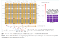
Despite these advantages, most of existing researches on 3D NAND-based CIM remain at an academic level, focusing on theoretical designs or small-scale prototypes, with little attention paid to system-level architecture design and functional validation using product-grade 3D NAND chips for LLM applications. To address this gap, we propose a novel CIM architecture based on 3D NAND flash, which utilizes a source line (SL) slicing technique to partition the array and perform parallel computation at minimal manufacturing cost. This architecture is complemented by an efficient mapping algorithm and pipelined dataflow, enabling system-level simulation and rapid industrial iteration.
We develop a PyTorch-based behavioral simulator for LLM inference on the proposed hardware, evaluating the influences of current distribution and quantization on system performance. Our design supports INT4/INT8 quantization and employs dynamic weight storage logic to minimize voltage switching overhead, and is further optimized through hierarchical pipelining to maximize throughput under hardware constraints.
Simulation results show that our simulation-grade 3D NAND compute-in-memory chip reaches generation speeds of 20 tokens/s with an energy efficiency of 5.93 TOPS/W on GPT-2-124M and 8.5 tokens/s with 7.17 TOPS/W on GPT-2-355M, respectively, while maintaining system-level reliability for open-state current distributions with σ < 2.5 nA; in INT8 mode, quantization error is the dominant accuracy bottleneck.
Compared with previous CIM solutions, our architecture supports larger model loads, higher computational precision, and significantly reduced power consumption, as evidenced by comprehensive benchmarking. The SL slicing technique keeps array wastage below 3%, while hybrid wafer-bonding integrates high-density ADC/TIA circuits to improve hardware resource utilization.
This work represents the first system-level simulation of LLM inference on product-grade 3D NAND CIM hardware, providing a standardized and scalable reference for future commercialization. The complete simulation framework is released on GitHub to facilitate further research and development. Future work will focus on device-level optimization of 3D NAND and iterative improvements of the simulator algorithm.​

1768591675344.png

Please, Log in or Register to view URLs content!
 

tokenanalyst

Lieutenant General
Registered Member

A domestic manufacturer of memory chip testing equipment has completed a nearly 100 million yuan Series B financing round!​


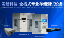
Luanqi Technology (Suzhou) Co., Ltd., a domestic manufacturer of memory chip testing equipment, has successfully completed a Series B financing round of nearly RMB 100 million, led by CAS Star, with follow-on investments from Hetang Capital and Yixin Capital. The funds will be used to expand production, boost R&D, and develop new product lines.

Founded in 2022, Luanqi Technology boasts a core team with over 10 years of experience at global semiconductor leaders such as AMD, Samsung, Huawei, and ZTE. The company specializes in NAND Flash-based storage testing technology, addressing the critical shortage of high-end domestic storage chip testing equipment.
1768599598413.png

It offers end-to-end testing solutions for SSDs, UFS, and NAND chips across R&D, production, and product introduction stages making it the only domestic provider covering all stages of semiconductor storage testing. Its products are already adopted by leading domestic and international players in storage, server, data center, and new energy vehicle sectors.

Please, Log in or Register to view URLs content!
 

tokenanalyst

Lieutenant General
Registered Member

Shanghai Science and Technology Innovation Board invests 692 million yuan in GELUN Electronics, marking a key leap forward for the domestic EDA ecosystem.​


Shanghai Science and Technology Innovation Group (SSEITC), a state-owned investment arm of Shanghai SDIC, has invested 692 million yuan in GELUN Electronics, acquiring a 5% stake at 31.80 yuan per share. This strategic move marks a significant boost for China’s domestic EDA ecosystem and signals strong institutional confidence in the company's long-term potential.

The investment deepens an existing strategic partnership established in July 2025 between GELUN Electronics and Shanghai SDIC, aimed at integrating resources to build a self-reliant semiconductor design platform. SSEITC’s participation through its extensive experience in tech innovation and industrial synergy provides both financial support and credibility, enhancing governance and stability as GELUN prepares for major restructuring.

GELUN has demonstrated strong financial performance and sustained R&D investment: operating revenue reached 315 million yuan in the first three quarters of 2025 (up 12.7% year-on-year), with net profit surging by over 170%. With more than 840 million yuan in cumulative R&D spending consistently accounting for over 60% of revenue it has established a solid technological foundation based on DTCO methodology, positioning it as a leader in high-end EDA tools.

As part of an upcoming 2.174 billion yuan asset restructuring, GELUN plans to acquire Ruicheng Microelectronics and Nanotech, transforming from a pure EDA tool provider into a “one-stop EDA+IP” chip design platform. This evolution could make it the first listed Chinese company to fully integrate EDA and semiconductor IP services, driving ecosystem development and strengthening China’s domestic semiconductor supply chain resilience.

Please, Log in or Register to view URLs content!
 

FriedButter

Brigadier
Registered Member
Please, Log in or Register to view URLs content!

Nvidia suppliers halt H200 output after China blocks chip shipments​

Suppliers of parts for Nvidia’s H200 chips, which recently gained US approval for sale in China, have paused production after local customs officials blocked shipments of the AI processors.

Makers of essential H200 components, such as the printed circuit board, have paused manufacturing following moves to prevent chip shipments entering China, according to two people with knowledge of the matter.

A customs ban, if sustained, would be a blow to Nvidia. The company has heavily lobbied Washington and Beijing to allow sales of its H200 chips, an older generation of AI processors, in China. After US President Donald Trump indicated he would permit sales last month, Nvidia began stepping up production.

The company had expected more than 1mn orders from Chinese clients, according to the people with knowledge of the matter. Its suppliers had been working around the clock to prepare for deliveries initially planned for as early as March.

However, Chinese customs officials on Tuesday summoned logistics companies in Shenzhen to tell them they could not submit customs clearance applications for H200 chips, one of the people said, though it was unclear if the ban was temporary.

The person added Nvidia was caught by surprise by the customs authorities’ move, which occurred as early shipments of H200s arrived in Hong Kong this week.

The regulatory uncertainty led Nvidia’s parts suppliers to pause production this week to avoid incurring inventory write-offs, the people said.

In the case of the printed circuit boards, they are specifically designed for H200 chips and cannot be used for other products, said Chu Wei-Chia, analyst at SemiAnalysis.

Beijing has been pushing tech companies to use domestic chips in a bid to achieve self-sufficiency in semiconductor production.

The FT previously reported that regulators were discussing ways to permit limited access to H200 chips, which tech giants such as Alibaba, ByteDance and Tencent prefer because of their higher performance and easier maintenance.

“The question of which government agency is regulating AI and the semiconductor industry in China is really complicated right now,” said George Chen, partner and co-chair of digital practice at The Asia Group.

“There are competing views between the [National Development and Reform Commission], the [Ministry of Industry and Information Technology] and the Cyberspace Administration of China about what role Nvidia should play, which is leading to a confusing mixture of policies.”

Potential restrictions being discussed include a licensing regime in which only companies with advanced AI model training needs can apply and a mandated ratio of domestic versus imported chips, said the people familiar with the matter.

Uncertainty around the H200 chip has also prompted many Chinese customers to reassess their options.

One Chinese seller of Nvidia AI servers said many local customers had cancelled orders for the H200. Instead, they have switched to the more advanced B200 and B300, which are banned for export into China by Washington, leading to an active black market for the chips.

This is not the first time Nvidia has faced restrictions from Chinese authorities. Last summer, Beijing stopped the country’s tech giants from purchasing the H20, a lower-performance version of the H200 designed to comply with US export controls.

Nvidia and China’s General Administration of Customs did not immediately respond to requests for comment.
 

gotodistance

New Member
Registered Member
China’s first tandem high-energy hydrogen ion implanter (POWER-750H), independently developed by the China Institute of Atomic Energy under the China National Nuclear Corporation, successfully generated a beam

Please, Log in or Register to view URLs content!


The POWER-750H, recently developed by China, is a high-energy hydrogen ion tandem implanter used in the manufacturing of power semiconductors (such as SiC/GaN).
Advanced logic chips at 5nm and below (e.g., smartphone APs) require low-energy ion implanters, which are supplied by overseas companies such as Axcelis and Applied Materials.
In other words, while the POWER-750H is unrelated to the 5nm process, it is significant in that it demonstrates China's progress in domestic production of power semiconductors.
The phrase "breakthrough in four key equipment" may be confusing, but ion implanters utilize completely different technologies for different applications.

from QWEN
 

sunnymaxi

Colonel
Registered Member
The POWER-750H, recently developed by China, is a high-energy hydrogen ion tandem implanter used in the manufacturing of power semiconductors (such as SiC/GaN).
Advanced logic chips at 5nm and below (e.g., smartphone APs) require low-energy ion implanters, which are supplied by overseas companies such as Axcelis and Applied Materials.
In other words, while the POWER-750H is unrelated to the 5nm process, it is significant in that it demonstrates China's progress in domestic production of power semiconductors.
The phrase "breakthrough in four key equipment" may be confusing, but ion implanters utilize completely different technologies for different applications.

from QWEN
these Ai tools are pretty useless.

in Low-energy category there are Three major Chinese companies providing solution up to 7nm as of now. Kaishitong , Sirui Intelligent and Huahai Qingke.

in fact, Huahai Qingke's launched first 12-inch low-energy ion implanter just recently.

Link -
Please, Log in or Register to view URLs content!


there are two more players in Logic ion implanter category. CETC provided upto 14nm and below. NAURA also entered in this sector.
 

tokenanalyst

Lieutenant General
Registered Member

Lianyong Microelectronics: Low-Earth Orbit satellite communication chips have been shipped in large quantities, and terrestrial communication terminal chips have passed customer verification.​


Recently, Lianyong Micro disclosed on its investor interaction platform that its subsidiary, Lianyong Dongxin, has mastered the industry's leading single-chip integration process technology. This technology can integrate functional modules such as power transistors with a gate length of 0.15 micrometers, low-noise transistors, PN diodes, E/D logic circuits, and RF switches into a single chip, and has already achieved commercial mass production.

The company stated that this integrated process, combined with other related technologies, enables the realization of power amplifiers and low-noise amplifiers with industry-leading performance on the same chip, with applications covering both satellite communication and terrestrial communication terminals.

According to Lion Microelectronics, chips developed based on this technology for low-orbit satellite communication have already been shipped in large quantities, while related chips for ground communication terminals have also passed customer verification and are ready for market promotion.

This advancement marks a significant breakthrough for Lion Microelectronics in the field of high-end radio frequency integrated circuits, and its technological capabilities and productization process are expected to be further expanded in emerging markets such as satellite communications and 5G communications.

Please, Log in or Register to view URLs content!
 
Top