You are using an out of date browser. It may not display this or other websites correctly.
You should upgrade or use an alternative browser.
You should upgrade or use an alternative browser.
Chinese semiconductor thread II
- Thread starter vincent
- Start date
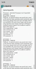
Jeez, I can't believe so many people in this forum do not even know the Android virtual machine on HarmonyOS called DroidTung. Let's stop posting shitty scores obtained in the virtual machine please and let's discuss something more constructive.This score is basically the same as the kirin 9000s. No progress in 2 years. Does not give a good outlook.
Something that's not Huawei or China, but still kind of interesting to consider when it comes to semi stuff.
All the US AI chips will now be forced to use Intel EMIB packaging instead of TSMC CoWoS and lose about 20% die in the process.
All the US AI chips will now be forced to use Intel EMIB packaging instead of TSMC CoWoS and lose about 20% die in the process.
Huawei: First time?Something that's not Huawei or China, but still kind of interesting to consider when it comes to semi stuff.
All the US AI chips will now be forced to use Intel EMIB packaging instead of TSMC CoWoS and lose about 20% die in the process.
Japan and most European countries are not ahead of China in the semiconductor field. Especially when considering IC design capabilities, the signs of decline in Japan's semiconductor industry over the past decade have been very obvious. Only semiconductor materials can still maintain a relatively strong competitiveness. South Korea is one of the leading countries in semiconductors.lol I don’t see why some of you guys are surprised. Europe has always been and will for the firseeebale future be on the side of the US when push comes to shove against any US advesary/rival. So I don’t think there’s anything surprising seeing the Dutch working hand in hand and even volunteering their largest and most advanced tech company to spy on China for the US for free. In fact China should assume that almost every European company will do or is doing the same. so it’s up to them to take their own measures to protect themselves . Geo politics is not a fairy tale lol you can’t blame others if you don’t take precautions to protect your secrets and tech. lol moreover, I don’t think Chinanjad a choice anyway to be honest, since they have been way behind the US/west/Japan/Taiwan in semiconductors, chips ,lithography etc for a long time, so even if they know they still had to keep relying on these machines to keep their products going despite the risks.
however things are slowly changing , so when they know they have caught up they will obviously reduce their reliance on the is companies products for a long time
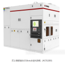
AMIES first 350nm stepper lithography machine from Chip-on-Micro was officially shipped.
Shanghai AMIES Semiconductor Manufacturing Co., Ltd. (AMIES), under its brand *Chip-on-Micro*, has successfully delivered its first independently developed 350nm stepper lithography machine, the AST6200, marking a major milestone in China’s pursuit of self-reliance in high-end semiconductor equipment.
AST6200 Stepper Lithography Machine
The AST6200 is a fully autonomous, high-performance, and high-precision stepper lithography system designed specifically for advanced compound semiconductor manufacturing including power devices, radio frequency (RF) front-ends, optoelectronics, and Micro LED displays.

Technical Features:
350nm Resolution: Achieved via a large numerical aperture projection lens and advanced illumination modes (variable pupil technology), enabling precise patterning for current mainstream compound semiconductor chips.
High Overlay Accuracy:
- 80nm front-side overlay
- 500nm back-side overlay
Ensures precision in multi-layer chip fabrication, improving device yield and reliability.
High Productivity & Efficiency:
High Productivity & Efficiency:
- High-intensity I-line (365nm) light source
- Fast linear motor system supporting rapid switching between substrate sizes (2", 3", 4", 6", 8")
- Motion table with up to 1.5g acceleration, boosting throughput and reducing cycle times.
Broad Process Flexibility:
- Compatible with diverse materials: Si, SiC, InP, GaAs, sapphire
- Supports various substrate types (flat edge, double flat edge, notch)
- Innovative multi-spot, wide-angle focusing system enables accurate alignment on transparent, translucent, and large-step substrates
- Back-side alignment module for complex bonding processes (e.g., wafer-level stacking)
Full Domestic Autonomy:
- 100% independently developed software stack from hardware drivers to process control enabling remote operation, real-time monitoring, and intelligent lifecycle management.
- Fully controllable, scalable system that supports future upgrades and integration into smart manufacturing ecosystems.
80nm overlay for 350nm is quite good. The overlay requirement for a 350nm process node is about 120nm, I expect them to reach KrF steppers pretty soon.
TCL CSOT increases investment in Optics Valley, signing an agreement to build a pilot-scale verification platform for "printed OLED".
TCL CSOT has signed a major agreement with the East Lake High-tech Development Zone to build a pilot-scale verification platform for printed OLEDs, investing approximately 1.5 billion yuan over 2025–2028. This expansion will increase monthly production capacity from 3,000 to 9,000 large cells, focusing on key upstream materials and equipment validation to accelerate industrialization.
TCL CSOT, a global leader in display technology with 2024 revenue of RMB 89.67 billion, has been active in Optics Valley since 2014, investing over 80 billion yuan and employing more than 17,000 people. It holds over 24,000 patent applications and nearly 10,000 authorized patents ranking first in Hubei for invention patents.
The project marks a significant step in China’s push for technological self-reliance in OLED displays, with printed OLED seen as a key pathway to leapfrog global competition. Optics Valley is now recognized as China's most advanced cluster for small and medium display production, and this initiative will strengthen its position as a global hub for display innovation and industrialization.
A project for high-end nanomaterials for integrated circuits and electronic components has been established in Dalian!
Dalian Jinpu New Area and Shanghai Huajujin New Materials Technology Co., Ltd. held a signing ceremony for a project on high-end integrated circuit and electronic component nano-functional materials.
Shanghai Huajujin New Materials Technology Co., Ltd.'s high-end integrated circuit and electronic component special nano-functional materials project is located in the Sanlibao Port Industrial Zone of Puwan Economic Zone, with a total investment of 500 million yuan.
The first phase of the project has a total investment of 130 million yuan, covering an area of approximately 10,000 square meters. It will construct 10 production lines for functional materials for integrated circuits, along with supporting facilities such as a pre-processing workshop for integrated circuit materials, a high-precision purification workshop, and an integrated circuit-level testing workshop. The project is designed to have an annual production capacity of 500 tons and an annual output value of 200 million yuan. The second phase of the project has a total investment of 370 million yuan and will construct a smart factory for high-end integrated circuit and electronic component-specific nanomaterials.
According to public information, Shanghai Huajujin New Materials Technology Co., Ltd. was established in 2022. The company's business revolves around non-ferrous metal alloys and related new materials, and also involves import and export trade.
Did you not read what the guy said after? Besides, it's not the full product, and it isn't in ideal conditions during the test either.This score is basically the same as the kirin 9000s. No progress in 2 years. Does not give a good outlook.

